11@ Finite-size-induced transition in ensemble of globally coupled oscillators
Simulink建模规范 3.0(MAAB)-11部分-14部分

11.附录A:模型检查工具开发(Recommendations for Automation Tools)该部分适用于开发模型检查工具的公司。
MathWorks汽车咨询委员会(MAAB)为使用MathWorks工具箱开发工具的供应商制定了这些建议,工具供应商应该根据该部分开发模型检查工具。
为了向工具的潜在用户提供最大限度的信息,建议工具供应商提供一个合规性矩阵(compliance matrix),该矩阵可在工具运行时轻松访问。
无需购买工具即可获得此信息。
合规矩阵应包括以下信息:⏹检查使用的指南版本●包括MAAB指南标题页上的完整标题(完整标题和版本号)。
⏹每条指南应该包括如下信息:●指南ID●指南标题●合规性等级●详情注:指南ID和标题应与指南中ID和标题完全一致。
合规性等级包括:纠正(Correction)–工具检查并自动或半自动纠正不合规项。
检查(Check)–工具检查并标记不合规项。
由软件开发人员纠正。
部分检查(Partial)–工具检查指南的部分规则。
细节部分应明确指出检查了哪部分规则和哪部分规则未检查。
无(None)–工具未检查指南。
对于未检查项,强烈建议供应商提供如何手动检查的方法。
12.附录B:指南制定(Guideline Writing)该部分适用于指定新的指南。
具有以下特征的指南易于理解和使用,因此,指定指南时至少应包括以下特征:●可理解且明确的(Understandable and unambiguous)●易于查找(Easy to find)●最小化(Minimal)可理解且明确的(Understandable and unambiguous):指南描述应准确、措辞清晰、简洁,并应定义模型(或模型的一部分)的属性特征。
小心地使用“必须”、“应当”、“应当”和“可以”等词;它们具有不同的含义,对模型开发人员和模型检查人员(人工和自动化)很重要。
如果指南作者描述了如何达到指南规范一致的操作(例如,通过选择特定选项或单击特定按钮),则对读者很有帮助。
沟道型折射率多模光纤的前向布里渊散射效应及其温度响应

Nov.2020Vol.37No.S Transactions of Nanjing University of Aeronautics and AstronauticsFBS Effect and Temperature Dependence in Trench⁃AssistedMultimode FiberZHANG Zelin1,2,LU Yuangang1,2*,XIE Youwen1,2,HUANG Jian1,2,ZHOU Lang1,2 1.Key Laboratory of Space Photoelectric Detection and Perception of Ministry of Industry and Information Technology,College of Astronautics,Nanjing University of Aeronautics and Astronautics,Nanjing211106,P.R.China;2.College of Science,Nanjing University of Aeronautics and Astronautics,Nanjing211106,P.R.China(Received13July2020;revised10September2020;accepted12September2020)Abstract:We propose the trench-assisted multimode fiber(TA-OM4)as a novel sensing fiber in forward Brillouin scattering(FBS)-based temperature sensor,due to its higher temperature sensitivity,better bending resistance and lower propagation loss,compared with the single mode fiber(SMF)and other sensing fibers.The FBS effect and acousto-optic interaction in TA-OM4are the first time to be demonstrated and characterized at1550nm theoretically and experimentally.A2.0km long TA-OM4is put into an oven to measure its temperature sensitivity,which can reach up to80.3kHz/℃,exceeding53%of SMF(52.4kHz/℃).The simulated and experimental results verify that the TA-OM4may be a good candidate as the sensing fiber for the FBS-based temperature sensor.Key words:forward Brillouin scattering;acousto-optic interaction;optic-fiber sensor;temperature sensitivity;multimode fiberCLC number:TN29Document code:A Article ID:1005‐1120(2020)S‐0095‐070IntroductionStimulated Brillouin scattering(SBS)in opti‐cal fiber is a phenomenon caused by the interaction between a light wave and an acoustic wave,which is widely studied and employed in the field of distrib‐uted sensing[1-2].Backward Brillouin scattering in‐duces high frequency shifts around10GHz which can be utilized in Brillouin optical time-domain sen‐sors and Brillouin laser.However,the forward Brill‐ouin scattering(FBS)have much lower frequency shift of several hundreds of mega Hertz,which can be used in several applications,such as temperature sensing,opto-mechanical chemical sensors,optical frequency comb and opto-mechanical laser[3-6].Recently,the temperature sensors based on FBS have been proposed using the silica single mode fiber(SMF),high nonlinear fiber(HNLF)and photonics crystal fiber(PCF)[7-9].However,the lower temperature sensitivity of SMF may limit its measurement pared with SMF,al‐though the HNLF and PCF have slightly lager tem‐perature sensitivities,their disadvantages of bad bending resistance,high cost and large propagation loss which are5.4dB/km of PCF and0.76dB/km of HNLF,respectively,can compromise their sens‐ing performance for future FBS-based temperature sensors in complex engineering application[8-9].For‐tunately,the trench-assisted multimode fiber(TA-OM4),due to its low propagation loss(0.24dB/ km)which is similar to that of SMF(0.20dB/ km),excellent bending resistance and high back‐ward stimulated Brillouin scattering(BSBS)and modulation instability(MI)threshold,has been a good candidate as the sensing fiber in BSBS-based temperature sensors[10].However,the characteristic of FBS process in TA-OM4at1550nm and its ap‐plications in FBS-based temperature sensors have*Corresponding author,E-mail address:*************.cn.How to cite this article:ZHANG Zelin,LU Yuangang,XIE Youwen,et al.FBS effect and temperature dependence in trench‐assisted multimode fiber[J].Transactions of Nanjing University of Aeronautics and Astronautics,2020,37(S):95‐101. http:///10.16356/j.1005‐1120.2020.S.012Vol.37 Transactions of Nanjing University of Aeronautics and Astronauticsnot been reported.In this paper,we theoretically and experimen‐tally investigate the acousto-optic interaction causedby FBS and FBS spectrum in TA-OM4.Further‐more,we have found that the largest strain coeffi‐cient in TA-OM4is about4.0kHz/με,which is sosmall that the frequency shift of FBS is not sensitiveto make acceptable strain measurement.Therefore,we only focus on its temperature dependence ofFBS in this pared with the temperatureresponse of FBS in SMF,we experimentally mea‐sure the FBS temperature response of TA-OM4.The highest temperature dependence of TA-OM4islinear with a coefficient of80.3kHz/℃,which is53%larger than that of SMF(52.4kHz/℃).Thesimulated and experimental results show that theTA-OM4may be a good candidate as the sensing fi‐ber in FBS-based temperature sensors.1FBS Resonances in TA⁃OM41.1Theoretical description of FBS in optical fi⁃berThe acoustic modes responsible for FBS are ra‐dial dilatational modes(R0,m)and mixed torsional-radial modes(TR2,m).The FBS is a typical opto-acoustic interaction,which can be described as thecoupling amplitude equations between optical fieldE(r,z,t)and acoustic wave for the displacementvector U(r,z,t)[11]∂2E ∂z2-n2effc2∂2E∂t2=1ε0c2∂2P NL∂t2(1)∂2U∂z2+Γ∂U∂t+V s2∇×(∇×U)-V l2∇(∇∙U)=Fρ(2) where P NL is the total nonlinear polarization,c the light velocity in vacuum,n eff the effective refractive index,ε0the vacuum permittivity,V l the longitudi‐nal acoustic velocity of the fiber,ρ0the density of fused silica,V s shear sound velocity of the fiber,andΓthe acoustic damping parameter.F=ε0[12γ12∇()E∙E+γ44(E∙∇)E]is the elec‐trostrictive driving term,andγ12andγ44are both the elements of the electrostrictive tensor for fused sili‐ca.By employing the finite element analysis(FEA)method and solving Eq.(1),we obtain the optical field E(r).Moreover,by solving Eq.(2)with the appropriate boundary conditions,we difine the nor‐malized displacement distribution U m(r)in terms of Bessel functions J n(z),where n is the order of Bes‐sel functions.By usingρm(r)=-ρ0∇U m(r),we obtain the density vibration caused by FBS.For the radial dilatational R0,m modes,the boundary condition corresponding to the free fiber surface can be written as(1-α2)J0(y)-α2J2(y)=0(3) whereαis the ratio between shear sound velocity and longitudinal acoustic velocity,and y m the m th zero of Eq.(3).Furthermore,the central frequency of the m th acoustic mode can be expressed asf m=y m V lπd(4) where d is the cladding diameter of optical fiber.Similar to the Kerr effect in fiber,the opto-me‐chanical coefficient can be used to quantify the opto-acoustic interaction caused by FBS,which can be expressed as[6,12-13]γ(m)OM=k02πn2neff cρ0Q(m)E Q(m)pΓm f m(5) whereΓm is the linewidth of the m th resonant peak induced by FBS.The Q(m)E and Q(m)p are the elec‐trostrictive overlap and photo-elastic overlap,which determines the efficiency of stimulation of acoustic modes and describes the modification of the effec‐tive index by acoustic modes[13-14],respectively.By solving Eqs.(1)—(5),the acoustic field distribu‐tion and FBS resonances can be obtained next.1.2Simulation and FBS spectrum in TA⁃OM4For TA-OM4,the diameters of the fiber core and cladding are50and125μm,respectively.The refractive index profile is given in Fig.1.The refrac‐tive index profile shows a quasi-quadratic distribu‐tion in the central region and has a trench-index pro‐file around the fiber core[10].The three highest linear polarization(LP)modes are respectively LP01,96No.S ZHANG Zelin,et al.FBS Effect and Temperature Dependence in Trench-Assisted Multimode FiberLP11and LP21,and the corresponding intensity ratio of these three LP modes I01∶I11∶I21,is1∶0.14∶0.006. Considering the highest intensity ratio of LP01,the tiny coupling efficiency between LP01and other high-order modes and the single mode condition of most optical components[15],it is enough to investigate the FBS process of TA-OM4corresponding to the fundamental mode LP01.By solving Eqs.(1)and(2),three excited acoustic modes are found and displayed in Fig.2. As it shown in Fig.2(a),taking R0,4mode as an example,the R0,m modes are the radial dilatational modes,which have the most efficient scattering ef‐ficiency and are independent of angular coordinate φ.Especially,the R0,m modes can induce refractive index changes so that the pure phase modulation will be also induced.Other acoustic modes are TR2,m acoustic modes,which are the mixed tor‐sional-radial modes.As it shown in Figs.2(b)and (c),different from R0,m modes,the TR2,m modes are doubly degenerated,which vary sinusoidally with angular coordinate2φ.Furthermore,the scat‐tering efficiency of TR2,m modes is much lower than that of R0,m modes.For the TR2,m(90°/0°)mode,its induced birefringent axes are parallel to the birefringent axes of TA-OM4,which does not induce the depolarized scattering but the polarized scattering and also cause pure phase modulation. For the TR2,m(45°/-45°)mode,the mode pat‐tern is rotated by45°.In this case pure phase modu‐lation will not occur,and the depolarized scattering is induced[16].Fig.1Refractive index profile of TA-OM4and calculated three LP optical modes with the highestintensityFig.2Normalized transverse profile of acoustic modes excited by LP01optical mode in TA-OM497Vol.37Transactions of Nanjing University of Aeronautics and Astronautics Generally ,the overlap between optical modes and acoustic modes determines the shape of FBS resonances.Taking four acoustic modes (R 0,1to R 0,4)as examples ,the 2D mode profiles of longitu‐dinal optical fundamental mode LP 01and four acous‐tic modes are displayed in Fig.3.In order to experimentally investigate the FBS process in TA -OM4,we also measure the FBS spectrum by using a coherent detection ,which isshown in Fig.4.The light source (NKT Photonics )is a 1550nm single -wavelength semiconductor la‐ser with linewidth 5kHz.The pump light propagat‐ing through the isolator (ISO )is split into two branches by a 50/50coupler.The upper branch used as the pump light is amplified by an erbium -doped fiber amplifier (EDFA ,Amonics ).A narrow bandpass filter (BPF ,AOS Photonics )with 3.5GHz bandwidth is used to eliminate the amplified spontaneous emission (ASE )noise induced by ED‐FA.A variable attenuator (VA )is utilized to adjust the input power level to protect fiber components.The pump light is launched into 2.0km long TA -OM4(YOFC )to obtain the FBS signal which beats with the reference light.Finally ,a 1.6GHz bandwidth photodetector (PD ,Thorlabs PDB480)is utilized to detect the beat signal ,which is ana‐lyzed by an electrical spectrum analyzer (ESA ,Tektronix RSA5126B )and used to obtain the FBS spectrum.In our experiment ,the incident light power is 11.2mW.The measured FBS spectrum is shown in Fig.5.The measured FBS spectrum includes two parts.One part is from the R 0,m modes and the other is from the TR 2,m modes.However ,due to the ran‐dom change of polarization states along the TA -OM4,the FBS intensities induced by TR 2,m modes are much lower than those of R 0,m modes.As it shown in Fig.5,we can find that the fourth resonant peak with the highest intensity locates at 173.1MHz.By solving Eq.(5),we obtain the calculated opto -mechanical coefficient of R 0,4mode as 5.25(W∙km )-1,which is slightly higher than that of SMF 5(W ∙km )-1[6].In Fig.6,two adjacent resonant peaksgenerated by R 0,m modes have equivalent frequency interval of 47.5MHz ,which can be verified by solv‐ing Eq.(4).It is obvious that ,whatever resonant peaks intensity and frequency shift ,the calculated and experimental results are in good agreement.The largest difference of normalized intensity be‐tween calculated and experimental results are less than 5%,which are from the error of the estimated fiberparameters.Fig.32-D profiles of optical mode LP 01and acoustic modes R 0,1to R0,4Fig.4Experimental setup of measuring the FBS spectrum of TA -OM4Fig.5The measured FBS spectrum of TA -OM498No.S ZHANG Zelin,et al.FBS Effect and Temperature Dependence in Trench -Assisted Multimode Fiber 2TemperatureResponse inTA⁃OM4In order to evaluate whether the TA -OM4can be used as the novel sensing fiber in FBS -based tem ‐perature sensors ,we put both TA -OM4and SMF into an oven to measure their temperature sensitivi‐ties of R 0,m modes ,and results are shown in Fig.7.Seven different temperatures between -10℃to 50℃are measured with a temperatures step of 10℃.It is obvious that the temperature sensitivities increase linearly with an increase in m value of R 0,m modes ,whose trends are in accordance with that in Ref.[17].The observed temperature coefficient of R 0,12in TA -OM4can reach 80.3kHz/℃,which is 53%larger than that of SMF (52.4kHz/℃).Furthermore ,we also obtain the temperature sensitivities of spectral peaks corresponding to R 0,4(f 4=173.1MHz )mode in TA -OM4and R 0,5(f 5=222.9MHz )mode in SMF ,which exhibit the high‐est resonance intensity of all peaks.In Fig.8,the calibration temperature coefficient of TA -OM4(αTA‐OM4)can reach 31.9kHz/℃,which is much 41%larger than that of SMF (αSMF =22.6kHz/℃).3ConclusionsFBS processes in TA -OM4are theoreticallyand experimentally investigated and the acousto -op‐tic interaction of TA -OM4at 1550nm are charac‐terized and demonstrated.We experimentally mea‐sure the FBS spectrum ,which is in good agreement with simulated results.The temperature sensitivities of R 0,m modes in TA -OM4are also measured ,which exceed 40%of SMF.The calculated and ex‐perimental results demonstrate that the TA -OM4could be a good sensing fiber in FBS -based tempera‐ture sensors ,with advantages of high temperature sensitivity ,good bending resistance and low propa‐gation loss.References[1]MATSUI T ,NAKAJIMA K ,YAMAMOTO F.Guided acoustic -wave brillouin scatteringcharacteris‐Fig.6Measured (green)and calculated (red)normal‐ized FBS resonant intensity in TA -OM4in‐duced by R 0,mmodesFig.7Measured temperature sensitivities of TA -OM4and SMF versus different R 0,m modes ,re‐spectivelyFig.8Temperature sensitivities of R 0,4mode in TA -OM4and R 0,5mode in SMF99Vol.37 Transactions of Nanjing University of Aeronautics and Astronauticstics of few-mode fiber[J].Applied Optics,2015,54(19):6093-6097.[2]BAO X,CHEN L.Recent progress in Brillouin scat‐tering based fiber sensors[J].Sensors,2011,11(4):4152-4187.[3]FU Y,FAN X,WANG B,et al.Discriminative mea‐surement of temperature and strain using stimulatedBrillouin scattering and guided acoustic-wave brillouinscattering[C]//2018Asia Communications and Photo‐nics Conference(ACPC).Hangzhou:IEEE,2018:1-3.[4]CHOW D M,THEVENAZ L.Opto-acoustic chemi‐cal sensor based on forward stimulated Brillouin scat‐tering in optical fiber(Invited)[C]//Proceedings ofthe7th International Conference on Photonics(ICP).[S.l.]:IEEE,2018:1-3.[5]BUTSCH A,KOEHLER J R,NOSKOV R E,et al.CW-pumped single-pass frequency comb genera‐tion by resonant optomechanical nonlinearity in dual-nanoweb fiber[J].Optica,2014,1(3):158-164.[6]LONDON Y,DIAMANDI H H,ZADOK A.Elec‐tro-opto-mechanical radio-frequency oscillator drivenby guided acoustic waves in standard single-mode fi‐ber[J].APL Photonics,2017,2(4):041303.[7]YAIR A,LONDON Y,ZADOK A.Scanning-free characterization of temperature dependence of forwardstimulated Brillouin scattering resonances[C]//Pro‐ceedings of the24th International Conference on Opti‐cal Fiber Sensors(ICOFS).Curitlba:SPIE,2015:96345C.1-96345C.4.[8]HAYASHI N,SUZUJI K,SET S Y,et al.Temper‐ature coefficient of sideband frequency produced by po‐larized guided acoustic-wave Brillouin scattering inhighly nonlinear fibers[J].Applied Physics Express,2017,10(9):092501.1-092501.3.[9]CARRY E,BEUGNOT J C,STILLER B,et al.Temperature coefficient of the high-frequency guidedacoustic mode in a photonic crystal fiber[J].AppliedOptics,2011,50(35):6543-6547.[10]ZHANG Z L,LU Y G.Trench-assisted multimode fi‐ber used in Brillouin optical time domain sensors[J].Optics Express,2019,27(8):11396-11405.[11]KANG M S,BRENN R,RUSSELL R S J.All-opti‐cal control of gigahertz acoustic resonances by forwardstimulated inter-polarization scattering in a photoniccrystal fiber[J].Physical Review Letters,2010,105(15):153901.1-153901.4.[12]BUTSCH A,KANG M S,EUSER T G,et al.Op‐tomechanical nonlinearity in dual-nanoweb structuresuspended inside capillary fiber[J].Physical ReviewLetters,2012,109(18):183904.1-183904.5.[13]DIAMANDI H H,LONDON Y,ZADOK A.Opto-mechanical inter-core cross-talk in multi-core fi‐bers[J].Optica,2017,4(3):289.[14]BIRYUKOV A S,SUKHAREV M E,DIANOV E M.Excitation of sound waves upon propagation of la‐ser pulses in optical fibers[J].Quantum Electronics,2002,32(9):765-775.[15]XU Y,REN M,LU Y,et al.Multi-parameter sensor based on stimulated Brillouin scattering in inverse-para‐bolic graded-index fiber[J].Optics Letters,2016,41(6):1138-1141.[16]NISHIZAWA N,KUME S,MORI M,et al.Experi‐mental analysis of guided acoustic wave Brillouin scat‐tering in PANDA fibers[J].Journal of the Optical So‐ciety of America B,1995,12(9):1651-1655.[17]CHUN Y D,SHANG L H,JING L L,et al.Simul‐taneous measurement on strain and temperature viaguided acoustic-wave Brillouin scattering in singlemode fibers[J].Acta Physica Sinica,2016,65(24).240702.1-240702.7.Acknowledgements This work was supported in part by the National Natural Foundation of China(Nos.61875086,61377086),the Aerospace Science Foundation of China (No.2016ZD52042),and Nanjing University of Aeronautics and Astronautics Ph.D.short-term visiting scholar project (No.190901DF08).Authors Mr.ZHANG Zelin is currently a Ph.D.candidate of Optical Engineering at the Department of Applied Phys‐ics,Nanjing University of Aeronantics and Astronautics (NUAA).His research focuses on distributed fiber sensors and nonlinear fiber optics.Prof.LU Yuangang is currently a professor in College of As‐tronautics at NUAA.His research focuses on distributed fi‐ber sensors,image processing and technology of photoelec‐trical detection.Author contributions Mr.ZHANG Zelin contributed to simulation by doing experiment and writing the manuscript. Prof.LU Yuangang designed and guided the study,and gave key opinions on the core issues.Mr.XIE Youwen and Mr.HUANG Jian conducted some related works about the experiments.Ms.ZHOU Lang conducted some related works about the simulation.Competing interests The author declare no competing interests.(Production Editor:XIA Daojia)100No.S ZHANG Zelin,et al.FBS Effect and Temperature Dependence in Trench-Assisted Multimode Fiber101沟道型折射率多模光纤的前向布里渊散射效应及其温度响应张泽霖1,2,路元刚1,2,谢有文1,2,黄剑1,2,周朗1,2(1.空间光电探测与感知工业和信息化部重点实验室,南京航空航天大学航天学院,南京211106,中国;2.南京航空航天大学理学院,南京211106,中国)摘要:提出了沟道型折射率多模光纤(TA‐OM4)可作为一种新型传感光纤应用于基于前向布里渊散射(FBS)的温度传感器中。
喷丸数值模拟中一种高效方法

表面技术第52卷第8期喷丸数值模拟中一种高效方法陈晟1,丁腾飞1,张朝阳2,高建永2,付婧颐1,鲁世红1(1.南京航空航天大学 机电学院,南京 210016;2.山东开泰抛丸机械股份有限公司,山东 滨州 256217)摘要:目的从减小分析步时间的角度出发,调整弹丸随机分布间距,研究提高模拟计算效率的方法。
方法以SAE1070弹簧钢为研究对象,在S230弹丸速度为40 m/s条件下,分析弹丸间垂直间距、水平间距和弹丸冲击方式对模拟结果的影响。
结果在不考虑弹丸间相互作用的前提下,有限元模拟中弹丸间可存在重叠,只要弹丸垂直间距大于0.07 mm,水平间距大于0.4 mm,弹丸随机生成模拟得到的诱导应力分布、塑性应变分布、粗糙度的结果在小偏差范围内收敛,与弹丸间无重叠的模拟结果相近。
在满足弹丸间距阈值的前提下,采用同时冲击和顺序冲击方式得到的诱导应力分布在压应力部分区域存在一定偏差,但应力分布曲线整体较为接近,同时冲击的计算时间缩短了约90%。
在此基础上,确定合适的弹丸分布,在不同弹丸直径、速度下进行阿尔门试片喷丸模拟,通过对比阿尔门强度值论证了模拟方法的有效性。
结论这种按层分布同时冲击,并在满足间距阈值的前提下尽可能减小间距的弹丸设置方法,保证了模拟精度,提高了计算效率,为数值模拟的应用提供了优化计算成本的新思路。
关键词:喷丸;数值模拟;SAE 1070;弹丸间距;诱导应力中图分类号:TG176 文献标识码:A 文章编号:1001-3660(2023)08-0458-08DOI:10.16490/ki.issn.1001-3660.2023.08.042An Efficient Approach in Numerical Simulation of Shot Peening CHEN Sheng1, DING Teng-fei1, ZHANG Chao-yang2, GAO Jian-yong2, FU Jing-yi1, LU Shi-hong1(1. College of Mechanical & Electrical Engineering, Nanjing University of Aeronautics and Astronautics, Nanjing 210016,China; 2. Shandong Kaitai Shot Blasting Machinery Share Co., Ltd., Shandong Binzhou 256217, China)ABSTRACT: Shot peening is a mechanical surface enhancement process widely used in the automotive and aerospace industry.The residual stress, as the main response parameter, plays an important role in improving the fatigue life of components.Compared with the costly and time-consuming experimental measurement, numerical simulation provides great convenience for the research of residual stress state, revealing mechanism and process optimization. Among them, the random multi-shot model can truly reflect the shot peening process, but it often faces the problem of high calculation cost, which limits the application of related technical methods. The shot peening model was established in Abaqus/Explicit in this paper. Therefore, from the perspective of increasing the spatial distribution density of shots to reduce the analysis step time, the distance and distribution收稿日期:2022-08-10;修订日期:2022-11-22Received:2022-08-10;Revised:2022-11-22作者简介:陈晟(1997—),男,硕士研究生。
PEER-REVIEWEDPUBLICATIONS
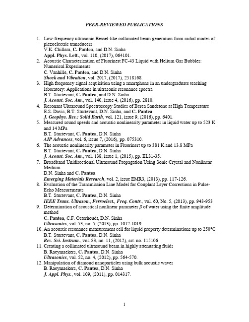
PEER-REVIEWED PUBLICATIONS1.Low-frequency ultrasonic Bessel-like collimated beam generation from radial modes ofpiezoelectric transducersV.K. Chillara, C. Pantea, and D.N. SinhaAppl. Phys. Lett., vol. 110, (2017), 064101.2.Acoustic Characterization of Fluorinert FC-43 Liquid with Helium Gas Bubbles:Numerical ExperimentsC. Vanhille, C. Pantea, andD.N. SinhaShock and Vibration, vol. 2017, (2017), 2518168.3.High frequency signal acquisition using a smartphone in an undergraduate teachinglaboratory: Applications in ultrasonic resonance spectraB.T. Sturtevant,C. Pantea, andD.N. SinhaJ. Acoust. Soc. Am., vol. 140, issue 4, (2016), pp. 2810.4.Resonant Ultrasound Spectroscopy Studies of Berea Sandstone at High TemperatureE.S. Davis, B.T. Sturtevant, D.N. Sinha, and C. PanteaJ. Geophys. Res.: Solid Earth, vol. 121, issue 9, (2016), pp. 6401.5.Measured sound speeds and acoustic nonlinearity parameter in liquid water up to 523 Kand 14 MPaB.T. Sturtevant,C. Pantea,D.N. SinhaAIP Advances, vol. 6, issue 7, (2016), pp. 075310.6.The acoustic nonlinearity parameter in Fluorinert up to 381 K and 13.8 MPaB.T. Sturtevant,C. Pantea,D.N. SinhaJ. Acoust. Soc. Am., vol. 138, issue 1, (2015), pp. EL31-35.7.Broadband Unidirectional Ultrasound Propagation Using Sonic Crystal and NonlinearMediumD.N. Sinha and C. PanteaEmerging Materials Research, vol. 2, issue EMR3, (2013), pp. 117-126.8.Evaluation of the Transmission Line Model for Couplant Layer Corrections in Pulse-Echo MeasurementsB.T. Sturtevant,C. Pantea,D.N. SinhaIEEE Trans. Ultrason., Ferroelect., Freq. Contr., vol. 60, No. 5, (2013), pp. 943-953 9.Determination of acoustical nonlinear parameter β of water using the finite amplitudemethodC. Pantea, C.F. Osterhoudt,D.N. SinhaUltrasonics, vol. 53, no. 5, (2013), pp. 1012-1019.10.An acoustic resonance measurement cell for liquid property determinations up to 250°CB.T. Sturtevant,C. Pantea,D.N. SinhaRev. Sci. Instrum., vol. 83, no. 11, (2012), art. no. 11510611.Creating a collimated ultrasound beam in highly attenuating fluidsB. Raeymaekers,C. Pantea,D.N. SinhaUltrasonics, vol. 52, no. 4, (2012), pp. 564-570.12.Manipulation of diamond nanoparticles using bulk acoustic wavesB. Raeymaekers,C. Pantea,D.N. SinhaJ. Appl. Phys., vol. 109, (2011), pp. 014317.13.High-pressure neutron diffraction studies at LANSCEY. Zhao, J. Zhang, H. Xu, K.A. Lokshin, D. He, J. Qian, C. Pantea, LL. Daemen, S.C.Vogel, Y. Ding, J. XuAppl. Phys. A: Mater. Sci. & Processing, vol. 99, no. 3, (2010), pp. 585-599.Special Issue: “Emerging Applications of Neutron Scattering in Materials Science and Engineering”14.Elastic constants of osmium between 5 and 300 KC. Pantea, I. Stroe, H. Ledbetter, J.B. Betts, Y. Zhao, L.L. Daemen, H. Cynn, A.MiglioriPhys. Rev. B, vol. 80, no. 2, (2009), pp. 024112-1-10.15.Bulk modulus of osmium, 4-300 KC. Pantea, I. Mihut, H. Ledbetter, J.B. Betts, Y. Zhao, L.L. Daemen, H. Cynn, A.MiglioriActa Mater., vol. 57, iss. 2, (2009) p. 544-54816.Diamond’s elastic stiffnesses from 322 K to 10 KA. Migliori, H. Ledbetter, R.G. Leisure, C. Pantea, J.B. BettsJ. Appl. Phys., vol. 104, no. 5, (2008), pp. 053512-1-417.Structure of diamond-silicon carbide nanocomposites as a function of sinteringtemperature at 8 GPaL. Balogh, S. Nauyoks, T. W. Zerda, C. Pantea, S. Stelmakh, B. Palosz, T. Ungar, Mat. Sci. Eng. A, vol. 487, no. 1-2, (2008), pp. 180-8.18.Direct measurement of spin correlation using magnetostrictionV.S. Zapf, V.F. Correa,P. Sengupta, C.D. Batista, M. Tsukamoto, N. Kawashima, P.Egan, C. Pantea, A. Migliori, J.B. Betts, M. Jaime, A. Paduan-FilhoPhys. Rev. B, vol. 77, no. 2, (2008), pp. 020404(R)-1-419.Osmium’s Debye temperatureC. Pantea, I. Stroe, H. Ledbetter, J.B. Betts, Y. Zhao, L.L. Daemen, H. Cynn, A.MiglioriJ. Phys. Chem. Solids, vol. 69, no. 1, (2008), pp. 211-213.20.High-Temperature Phase Transitions in CsH2PO4 under Ambient and High-PressureConditions: A Synchrotron X-ray Diffraction StudyC.E. Botez, J.D. Hermosillo, J. Zhang, J. Qian, Y. Zhao, J. Majzlan, R.R. Chianelli, C.PanteaJ. Chem. Phys., vol. 127, (2007), pp. 194701-1-621.Alpha-plutonium’s polycrystalline elastic constants over its full temperature rangeA. Migliori, C. Pantea, H. Ledbetter, J.B. Betts , J. E. Mitchell, M. Ramos, F. Freibert,D. Dooley, S. Harrington, C. MielkeJ. Acoust. Soc. Am., vol. 122, no. 4, (2007), pp. 1994-2001.22.Temperature and time-dependence of the elastic moduli of Pu and Pu-Ga alloysA. Migliori, I. Mihut, J.B. Betts, M. Ramos,C. Mielke, C. Pantea,D. MillerJ. Alloy. Compd., vol. 444-445, (2007), pp. 133-137.23.Investigation of relaxation of nanodiamond surface in real and reciprocal spacesB. Palosz,C. Pantea, E. Grzanka, S. Stelmakh, Th. Proffen, T.W. Zerda, W. PaloszDiam. Relat. Mater., vol. 15, no. 11-12, (2006), pp. 1813.24.Microstructure of diamond-SiC nanocomposites determined by X-ray line profileanalysisJ. Gubicza, T. Ungar, Y. Wang, G.A. Voronin, C. Pantea, T.W. ZerdaDiam. Relat. Mater., vol. 15, no. 9, (2006), pp. 1452.25.Pressure-induced elastic softening of monocrystalline zirconium tungstate at 300 KC. Pantea, A. Migliori, P. B. Littlewood, Y. Zhao, H. Ledbetter, J. C. Lashley, T.Kimura, J. Van Duijn, and G. R. KowachPhys. Rev. B, vol. 73, no. 21, (2006), art. no. 214118.26.Evidence for a Structural Transition to a Superprotonic CsH2PO4 Phase Under HighPressureC. E. Botez, R. R. Chianelli, J. Zhang, J. Qian, Y. Zhao, J.Majzlan, C. Panteain Materials in Extreme Environments, edited by C. Mailhiot, P.B. Saganti, D. Ila(Mater. Res. Soc. Symp. Proc.929E, Warrendale, PA, 2006), 0929-II02-01.27.Digital ultrasonic pulse-echo overlap system and algorithm for unambiguousdetermination of pulse transit timeC. Pantea,D.G. Rickel, A. Migliori, J. Zhang, Y. Zhao, S. El-Khatib, R.G. Leisure, B. LiRev. Sci. Instrum., vol. 76, no. 11, (2005), art. no. 11490228.Kinetics of the reaction between diamond and silicon at high pressure and temperatureC. Pantea, G.A. Voronin, T.W. ZerdaJ. Appl. Phys., vol. 98, no. 7, (2005), art. no. 073512.29.Kinetics of SiC formation during the high P-T reaction between diamond and siliconC. Pantea, G.A. Voronin, T.W. Zerda, J. Zhang, L. Wang, Y. Wang, T. Uchida, Y. ZhaoDiam. Relat. Mater., vol. 14, no. 10, (2005), pp. 1611.30.Experimental Constraints on the Phase Diagram of Zirconium MetalJ. Zhang, Y. Zhao, C. Pantea, J. Qian, L.L. Daemen, P.A. Rigg, R.S. Hixson, C.W.Greeff, G.T. Gray III, Y. Yang, L. Wang, Y. Wang, T. UchidaJ. Phys. Chem. Solids, vol. 66, (2005), pp. 1213.31.Thermal equations of state of α, β, and ω phases of zirconiumY. Zhao, J. Zhang, C. Pantea, J. Qian, L.L. Daemen, P.A. Rigg, R.S. Hixson, G.T. Gray III, Y. Yang, L. Wang, Y. Wang, T. UchidaPhys. Rev. B, vol. 71, no. 18,(2005), pp. 184119.32.Yield Strength of α-Silicon Nitride at High Pressure and High TemperatureJ. Qian, C. Pantea, J. Zhang, L.L. Daemen, Y. Zhao, M. Tang, T. Uchida, Y. Wang J. Am. Ceram Soc., vol. 88, no. 4, (2005), pp. 903.33.Microstructure of nanocrystalline diamond powders studied by powder diffractometryB. Palosz, E. Grzanka,C. Pantea, T.W. Zerda, Y. Wang, J. Gubicza, T. UngarJ. Appl. Phys., vol. 97, no. 6, (2005), pp. 064316.34.Thermal equation of state of osmium: a synchrotron x-ray diffraction studyG.A. Voronin, C. Pantea, T.W. Zerda, L. Wang, Y. ZhaoJ. Phys. Chem. Solids, vol. 66 , no. 5, (2005), pp. 706.35.Size and shape of crystallites and internal stresses in carbon blacksT. Ungar, J. Gubicza, G. Tichy, C. Pantea, T.W. ZerdaCompos Part A-Appl S, vol. 36, (2005), pp. 431.36.Structural influence of erbium centers on silicon nanocrystal phase transitionsR.A. Senter, C. Pantea, Y. Wang, H. Liu, T.W. Zerda, J.L. CofferPhys. Rev. Lett., vol. 93, no. 17, (2004), pp. 175502.37.Graphitization of diamond of different sizes at high pressure-high temperatureJ. Qian, C. Pantea, J. Huang, T.W. Zerda, Y. ZhaoCarbon, vol. 42, no. 12-13, (2004), pp. 2691.38.High pressure effect on dislocation density in nano-size diamond crystalsC. Pantea, J. Gubicza, T. Ungar, G.A. Voronin, N.H. Nam, T.W. ZerdaDiam. Relat. Mater., vol. 13, no. 10, (2004), pp. 1753.39.Powder Neutron Diffraction of Wustite (Fe0.93O) to 12 GPa using large moissaniteanvilsJ. Xu, Y. Ding, S.D. Jacobsen, H.K. Mao, R.J. Hemley, J. Zhang, J. Qian, C. Pantea, S.C. Vogel, D.J. Williams, Y. ZhaoHigh Press. Res., vol. 24, no. 2, (2004), pp. 247.40.Enhancement of fracture toughness in nanostructured diamond-SiC compositesY. Zhao, J. Qian, L.L. Daemen, C. Pantea, J. Zhang, G.A. Voronin, T.W. ZerdaAppl. Phys. Lett., vol. 84, no. 8, (2004), pp. 1356.41.In situ x-ray diffraction study of silicon at pressures up to 15.5 GPa and temperatures upto 1073 KG.A. Voronin, C. Pantea, T.W. Zerda, L. Wang, Y. ZhaoPhys. Rev. B, vol. 68, no. 2, (2003), pp. 020102.42.In situ x-ray diffraction study of germanium at pressures up to 11GPa and temperaturesup to 950KG.A. Voronin, C. Pantea, T.W. Zerda, J. Zhang, L. Wang, Y. ZhaoJ. Phys. Chem. Solids, vol. 64, no. 11, (2003), pp. 2113.43.Dislocation density and graphitization of diamond crystalsC. Pantea, J. Gubicza, T. Ungar, G.A. Voronin, T.W. ZerdaPhys. Rev. B, vol. 66, no. 9, (2002), pp. 094106.44.Microstructure of carbon blacks determined by X-ray diffraction profile analysisT. Ungar, J. Gubicza, G. Ribarik, C. Pantea, T.W. ZerdaCarbon, vol. 40, no. 6, (2002), pp. 929.45.High pressure study of graphitization of diamond crystalsC. Pantea, J. Qian, G.A. Voronin,T.W. ZerdaJ. Appl. Phys., vol. 91, no.4, (2002), pp. 1957.46.Oriented growth of b-SiC on diamond crystals at high pressureG. Voronin, C. Pantea, T.W. ZerdaJ. Appl. Phys., vol. 91, no.4, (2002), pp. 1957.47.Partial graphitization of diamond crystals under high-pressure and high-temperatureconditionsJ. Qian, C. Pantea, G. Voronin, T.W. ZerdaJ. Appl. Phys., vol. 90, no. 3, (2001), pp. 1632.48.Structure of carbon blacksT.W. Zerda, J. Qian, C. Pantea, T. UngarMat. Res. Soc. Symp. Proc., vol. 661, (2001), pp. KK6.4.1.49.A study on the electrodic process by Electrochemical Impedance Spectroscopy(Studiul procesului electrodic prin Spectroscopie de Impedanta Electrochimica)F. Kormos, L. Sziraki, C. PanteaRev Chim-Bucharest, vol. 51, no. 4, (2000), pp. 415.50.Enzimatic determination of urea in animal-origin whole blood and blood serum(Determinarea enzimatica a ureei din sange integral si ser sanguin de provenienta animala)I. Tarsiche, F. Kormos, C. PanteaRev Chim-Bucharest, vol. 51, no. 1, (2000), pp. 8.51.Redox sensors based on semiconductor film(Félvezetõ redoxi szenzor)F. Kormos, C. PanteaMagy. Kem. Foly., vol. 105, no. 9, (1999), pp. 379.52.Raman spectroscopic investigations of the xCuO·(1-x)[3B2O3·K2O] glassesD. Maniu, I. Ardelean, T. Iliescu, C. PanteaJ. Mater. Sci. Lett., vol. 16, (1997), pp. 19.BOOK CHAPTERDevelopment of high P-T neutron diffraction at LANSCEY. Zhao, D. He, J. Qian, C. Pantea, K.A. Lokshin, J. Zhang, L.L. Daemenin Advances in High-Pressure Technology for Geophysical Applications, Elsevier, pp.461-474, 2005LANL INTERNAL PUBLICATIONFilling the Gap in Plutonium Properties. Studies at Intermediate Temperatures andPressuresA. Migliori, A.J. Hurd, Y. Zhao and C. PanteaLos Alamos Science, vol. 30, (2006), pp. 86-89.PATENTS1.Apparatus and method for visualization of particles suspended in a fluid and fluid flowpatterns using ultrasound - European Patent EP2612113, Nov 16, 20162.Apparatus and method for acoustic monitoring of steam quality and flow – United StatesPatent US 9,442,094, Sep 13, 20163.Acoustic source for generating an acoustic beam – United States Patent US 9,354,346,May 31, 20164.Device and method for generating a collimated beam of acoustic energy in a borehole -European Patent EP2577357, Sep 02, 20155.System and method for sonic wave measurements using an acoustic beam source - UnitedStates Patent US 9,103,944, Aug 11, 20156.Device and method for generating a collimated beam of acoustic energy in a borehole -European Patent EP2577358, Jun 17, 20157.Device and method for generating a beam of acoustic energy from a borehole, andapplications thereof - European Patent EP2297595, May 21, 20148.Device and method for generating a beam of acoustic energy from a borehole, andapplications thereof - United States Patent US 8,559,269, Oct 15, 20139.Device and method for generating a beam of acoustic energy from a borehole, andapplications thereof - United States Patent US 8,547,791, Oct 1, 201310.Device and method for generating a beam of acoustic energy from a borehole, andapplications thereof - United States Patent US 8,547,790, Oct 1, 201311.System for generating a beam of acoustic energy from a borehole, and applicationsthereof - United States Patent US 8,259,530, Sep 4, 201212.System for generating a beam of acoustic energy from a borehole, and applicationsthereof - United States Patent US 8,233,349, Jul 31, 20113.Device and method for generating a beam of acoustic energy from a borehole, andapplications thereof - United States Patent US 7,839,718, Nov 23, 2010.CONFERENCE PROCEEDINGS1.Broad-band acoustic low frequency collimated beam for ultrasonic imagingC. Pantea,D.N. SinhaProceedings of Meetings on Acoustics (POMA), vol. 19, (2013), pp. 045058.2.Broadband directional ultrasound propagation using sonic crystal and nonlinear mediumD.N. Sinha, C. PanteaProceedings of Meetings on Acoustics (POMA), vol. 19, (2013), pp. 065047.3.Determination of the Acoustic Nonlinearity Parameter in Liquid Water up to 250°C and14 MPaB.T. Sturtevant,C. Pantea,D.N. SinhaProc. 2012 IEEE Int'l Ultrason. Symp., pp. 285-288.4.Acoustic Nonlinearity in Fluorinert FC-43C. Pantea,D.N. Sinha, C.F. Osterhoudt, P.C. MombourquetteProceedings of Meetings on Acoustics (POMA), vol. 6, (2009), pp. 045005-1-14.5.Nano-Diamond compressibility at pressures up to 85 GPaC. Pantea, J. Zhang, J. Qian, Y. Zhao, A. Migliori, E. Grzanka, B. Palosz, Y. Wang,T.W. Zerda, H. Liu, Y. Ding, P.W. Stephens and C.E. BotezTechnical Proceedings of the 2006 Nanotechnology Conference and Trade Show, Vol.1, (2006), pp. 823-826.PRESENTATIONS1.Ultrasonic techniques for measuring physical properties of fluids in harsh environmentsC. PanteaKeithley Award Session, APS March Meeting 2016, Baltimore, MD, 14-18 Mar 20162.Nuclear material identification using resonant ultrasound spectroscopyC. Pantea, T.A. Saleh, A. Migliori, J.B. Betts, E.P. Luther,D.B. Byler167th Meeting of the Acoustical Society of America, Providence, RI, 5-9 May 20143.Broad-band Acoustic Low Frequency Collimated Beam for Ultrasonic ImagingC. Pantea andD.N. Sinha21st International Congress on Acoustics, ICA 2013, Montreal, Canada, 2-7 June 20134.Acoustical Filters and Nonlinear Acoustic Wave Propagation in LiquidsC. Pantea andD.N. Sinha161st Meeting of the Acoustical Society of America, Seattle, WA, 23-27 May 20115.Acoustical shock formation in highly nonlinear fluidsC. Pantea andD.N. SinhaJoint 159th ASA Meeting and Noise-Con 2010, Baltimore, MD, 19-23 April 20106.Nonlinear Acoustical Beam Formation and Beam Profiles in FluidsC. Pantea andD.N. Sinha158th Meeting of the Acoustical Society of America, San Antonio, TX, 26-30 Oct 20097.Acoustic Nonlinearity in Fluorinert FC-43C. Pantea,D.N. Sinha, C.F. Osterhoudt, P.C. Mombourquette157th Meeting of the Acoustical Society of America, Portland, OR, 18-22 May 20098.Acoustic nonlinear beam formation and imagingC. PanteaTexas Christian University, Department of Physics and Astronomy, Fort Worth, TX, January 23, 20099.Negative-thermal-expansion ZrW2O8. Elasticity and pressure.C. Pantea, A. Migliori, P. B. Littlewood, Y. Zhao, H. Ledbetter, J. C. Lashley, T.Kimura, J. Van Duijn, and G. R. KowachAPS March Meeting 2007, March 5-9, Denver, CO.10.Osmium’s full elastic tensor between 5K and 300KC. Pantea152nd Meeting (4th joint meeting of the Acoustical Society of America and the Acoustical Society of Japan), Honolulu, Hawaii, 28 November-2 December 200611.Pressure-induced elastic softening of monocrystalline zirconium tungstate at 300KC. PanteaMSCookies and Tea, LANL, August 2nd, 200612.Nano-Diamond compressibility at pressures up to 85 GPaC. Pantea, J. Zhang, J. Qian, Y. Zhao, A. Migliori, E. Grzanka, B. Palosz, Y. Wang,T.W. Zerda, H. Liu, Y. Ding, P.W. Stephens and C.E. BotezNSTI Nanotech 2006, May 7-11, Boston, MA.13.Digital ultrasonic pulse-echo overlap system and algorithm for unambiguousdetermination of pulse transit timeC. Pantea,D.G. Rickel, A. Migliori, J. Zhang, Y. Zhao, S. El-Khatib, R.G. Leisure, B. LiAPS March Meeting 2006, March 13-17, Baltimore, MD.14.Unusual compressibility in the negative-thermal-expansion material ZrW2O8C. Pantea, A. Migliori, P. B. Littlewood, Y. Zhao, H. Ledbetter, T. Kimura, J. VanDuijn, G. R. KowachICAM/I2CAM Annual Conference on Frontiers in Complex Adaptive Matter & Satellite EventsNovember 8-12, 2005, Bishop's Lodge, Santa Fe, NM15.Nano-Diamond compressibility at pressures up to 85 GPaC. Pantea, J. Zhang, J. Qian, Y. Zhao, B. Palosz, T.W. ZerdaStewardship Science Academic Alliances (SSAA) Program SymposiumMarch 29-31, 2004, Albuquerque, NM.16.Phase-coherent pulse-echo ultrasound in a SiC anvil pressure cellC. Pantea,D.G. Rickel, R.G. Leisure, A. Migliori, Y. ZhaoStewardship Science Academic Alliances (SSAA) Program SymposiumMarch 29-31, 2004, Albuquerque, NM.17.Diamond Composites and control of graphitizationC. Pantea, J. Qian, G.A. Voronin, T.W. Zerda, Y. ZhaoIndustrial Materials For The Future (IMF), Annual Review MeetingJune 23-25, 2003, Golden, CO.18.Structure Study of Diamond-SiC Composites Obtained Under High Pressure-HighTemperature ConditionsC. Pantea, G.A. Voronin, T.W. Zerda, J. Qian, Y. ZhaoAPS March Meeting 2003, March 3-7, Austin, TX.19.Diamond-silicon reaction under high pressure - high temperature conditionsC. Pantea, G.A. Voronin, T. W. ZerdaMRCEDM Research Festival 2002, April 5, UTA, Arlington, TX.20.β-SiC formation on diamond crystals under high pressure-high temperature conditionsC. Pantea, G.A. Voronin, T. W. ZerdaTSAPS Fall Meeting 2001, October 4-6, TCU, Fort Worth, TX.21.X-ray diffraction study of diamond-graphite phase transition at high pressures andtemperaturesC. Pantea, J. Qian, T. W. ZerdaTSAPS Fall Meeting 2000, October 27-29, Rice University, Houston, TX.。
半导体纳米晶体介电常数的尺寸和成分效应

半导体纳米晶体介电常数的尺寸和成分效应马艳丽; 李明【期刊名称】《《淮北师范大学学报(自然科学版)》》【年(卷),期】2019(040)003【总页数】5页(P12-16)【关键词】介电常数; 半导体纳米晶体; 尺寸和成分效应【作者】马艳丽; 李明【作者单位】淮北师范大学物理与电子信息学院安徽淮北 235000【正文语种】中文【中图分类】O3410 引言由于低维纳米晶体(纳米粒子、纳米线、薄膜)具有不同于相应块体材料的物理化学性能,因此具有广泛的应用价值,从而引起学者们的广泛关注[1].介电常数ε是用来描述单元电荷产生电流的多少,作为一个重要的光电性能,学者们通过理论和实验方法对其进行广泛的研究[2].由于纳米材料约束电子的低屏蔽性,其介电常数小于相应的块体材料,即:ε(D)<ε(∞)[3-5].其中:D是纳米粒子和纳米线的直径、薄膜的厚度,∞则表示相应的块体材料.ε(D)的减小可以提高纳米器件中的电子、空穴和浅层杂质电离的库仑相互作用,并且改善光吸收和传输性能[2].比如:纳米闪存,纳米晶体通常是嵌入到栅极氧化物中作为一个电荷存储节点,纳米晶体的存在会对栅极电容产生影响[6-8].为得到所需性能的器件,首先要理解介电常数的基本原理.为得到所需的光电性能,大多数工作是通过改变尺寸来调整纳米晶体的介电常数,但在小尺寸范围内,尤其当尺寸下降到2~3 nm时,器件将不可避免地出现热稳定性问题[9].为解决小尺寸器件的热稳定性问题,可以用热稳定性高的多元合金[9],多元合金不仅具有相应的单相纳米晶体所具有的基本光电性能,同时还具有高的光致发光性能[10].为了描述ε(D),学者们在理论方面建立不同的模型,模型预测结果与实验结果保持一致,但模型中用到的可调参数限制了模型的应用[2,11].此外,由于对合金介电常数的成分效应研究很少,因此有必要建立一个定量的模型来描述介电常数的尺寸和成分效应.本文中,根据已建立的热力学模型,建立一个没有任何可调参数的模型来预测纳米晶体的介电常数.根据这个模型,对于化合物和合金,介电常数随着尺寸D的减小而减小.此外,通过选择适当的x,可以有效地对合金的ε(x,D)进行调整.通过与实验结果的比较证实模型的有效性,表明该模型可以为光电器件的开发、应用提供有效途径.1 模型根据近自由电子方法,Eg=2|V1|.其中:Eg是决定材料导电性能的带隙,V1是晶体场,取决于原子总数和固体原子间的相互作用[12].作为一级近似,将这种关系扩展到纳米尺寸,可以得到:其中Δ 表示差值,由于V∝Ec[12],Ec是原子结合能. 因此Ec(D)的函数可以表示为[13]:其中:Tm是熔化温度,Svib(∞)是振动熵,R是理想气体常数. 对于半导体,Svib(∞)≈Sm(∞)-R ,其中:Sm(∞)为熔化熵[14],D0是临界直径,此时低维材料中所有原子都位于表面.作为维数d和最近邻原子间距h的函数,D0可表示为[14]:其中d=0,1,2分别表示纳米粒子、纳米线和薄膜.介电常数来源于从价带到导带的电子极化或者电子跃迁过程.这个过程服从能量和动量守恒,并影响半导体的光电响应以及价带电子与激发的导带电子的耦合程度[2].因此,在室温下,半导体的介电常数与带隙Eg是直接相关的. 根据公式(1)~(3)以及的近似关系[2],尺寸依赖的磁化系数χ(D)可以表示为[χ(D)/χ(∞)]={2-[Tm(D)/Tm(∞)]}-2. 将ε=χ+1扩展到纳米尺寸,ε(D)可表示为对于纳米半导体合金,由于成分x对h(x)和Svib(x)产生影响,随着尺寸D的增加,ε(x,D)随成分的变化由直线变为曲线,表现出非线性关系.根据Fox方程h(x)和Svib(x)可表示为[15]:其中:Svib(0)、Svib(1)、h(0)和h(1)表示x=0或x=1时对应的块体值.表1 模型计算过程中用到的相关参数注aSvib(∞)∝Sm(∞)-R,其中:CdTe、CdSe的Sm(∞)分别是14.91 J/(g-atom·K)[18]、20.37 J/(g-atom·K)[18].CdSe CdTe ε(∞)[17]9.7 10.2 Svib(∞)/(J/(g-atom·K))6.59a 12.06ah[16]/nm 0.263 0.2812 结果与讨论计算中使用的参数如表1所示.图1是根据式(5)预测的CdTe和CdSe纳米粒子、纳米线的ε(D)与Tsu模型以及实验结果的比较.模型预测结果表明,随着尺寸D的减小,表面体积比(A/V)增大,ε(D)减小,模型预测结果和实验结果在整个范围内具有良好的一致性.而且,当纳米线的尺寸D<5 nm以及纳米粒子的尺寸D<10 nm时,ε(D)随着尺寸的变化变化明显;而当尺寸D>10 nm时,ε(D)随着尺寸的变化平缓,直至慢慢接近块体值.由于表面原子具有与内部原子不同的物理特性,随着尺寸的减小,表面体积比和表面原子数增多,因此,在决定纳米晶体的性能时,表面原子起主导作用.Wang等[5]提出介电常数的变化是由于表面的量子点而并不是所有的量子点,而Delerue等[3]认为,介电常数的减小是由表面极化键的断裂导致的,这正好支持Wang等的早期发现.研究表明,纳米晶体尺寸D 的减小导致晶格收缩和结合能减小[2].尽管晶格收缩会使单键能增加,但表面原子的低配位数(存在于表面的断裂建)导致纳米晶体的结合能随着表面原子的增大而减小.因此,配位数的缺失(结合能减小)导致可捕获到的哈密顿总量的改变,使得带隙增大,进而影响电子极化过程[19].根据以上分析以及介电常数和带隙的近似关系,ε(D)随着尺寸D的减小而减小是合理的.从图1还可以看出,纳米线介电常数的尺寸效应弱于纳米粒子.这种差异产生的原因是由于纳米粒子、纳米线的表面体积比分别是6/D、4/D.模型预测结果表明,可以通过改变尺寸来调节纳米合金的介电常数.相反,图1中Tsu的模型仅在D>10 nm时和实验结果存在一致性,而D<10 nm时,Tsu模型与实验结果存在偏差,这是由于Tsu的模型限定ΔEg(D)/Eg(∞)<0.56[11].实际上D<10 nm时,纳米晶体的ΔEg(D)/Eg(∞)值可以大于0.5[2].与Tsu的模型相比,模型预测的CdTe和CdSe纳米粒子、纳米线的ε(D)和实验结果有着良好的一致性.图1 模型预测的CdSe和CdTe的介电常数和Tsu模型以及实验结果的比较□[17]表示CdTe纳米线的实验结果;▼[20]、●[21]、◆[22]表示CdTe纳米粒子的实验结果;■[22]☆[23]表示CdSe纳米粒子的实验结果.图2 模型预测的CdSexTe1-x纳米合金的介电常数■、▲[24]表示实验结果图2是根据式(7)预测的不同尺寸的CdSexTe1-x的ε(x,D)随成分变化与实验结果的比较.从图2可以看出,一方面,对于固定的x,随着尺寸的变化,纳米合金的介电常数与化合物具有相同的变化趋势,即ε(x,D)随着D的减小而减小.另一方面,随着尺寸D的增加,纳米半导体合金的ε(x,D)随成分的变化由线性变成非线性,其介电常数随着尺寸D的增加表现出弯曲行为.D=4.9 nm时,ε(x,D)表现出近似线性关系,而D=14 nm时,ε(x,D)表现出非线性关系,而且随着D的增加弯曲行为越明显.当D增加到大尺寸范围时,比如D=40 nm和D=50 nm,ε(x,40)和ε(x,50)之间的差异很小,其介电常数接近于块体值,表明此时介电常数具有弱的尺寸效应.模型预测和实验结果的一致性证实该模型的有效性,并表明利用Fox方程来确定纳米半导体合金的热力学常数是合理的.值得一提的是,式(5)和式(8)只适用于具有自由表面或位于惰性基体的纳米晶体[24-27].对于通过气相沉积方法来制备的纳米晶体[9]与基底形成非共格、半共格和共格界面,这可能会导致不同的变化趋势,比如对于具有不同界面的纳米晶体,可能产生过冷或过热现象[13].因此,界面效应在以后的工作中会进一步进行讨论.3 结论通过已建立的熔化温度模型以及Fox方程,建立一个没有任何可调参数的热力学模型来预测半导体化合物和合金的ε(x,D).模型预测结果表明,纳米晶体的ε(x,D)随着尺寸D的减小而减小,纳米半导体合金的ε(x,D)随成分表现出弯曲行为.而且,由于表面体积比的不同,纳米粒子ε(x,D)的尺寸效应强于纳米线.模型预测结果和实验结果一致性表明模型的有效性和普适性,同时该模型为光电器件的开发、应用提供有效指导.参考文献:【相关文献】[1]CANHAM L T.Silicon quantum wire array fabrication by electrochemical and chemical dissolution of wafers[J].Applied Physics Letters,1990,57(10):1046-1048. [2]SUN C Q,SUN X,TAY B,et al.Dielectric suppression and its effect on photoabsorption of nanometric semiconductors[J].Journal of Physics D:Applied Physics,2001,34(15):2359.[3]DELERUE C,LANNOO M,ALLAN G.Concept of dielectric constant for nanosized systems[J].Physical Review B,2003,68(11):115411.[4]YOO H G,FAUCHET P M.Dielectric constant reduction in silicon nanostructures [J].Physical Review B,2008,77(11):115355.[5]WANG L W,ZUNGER A.Pseudopotential calculations of nanoscale CdSe quantum dots[J].Physical Review B,1996,53(15):9579.[6]DE SOUSA J S,PEIBST R,ERENBURG M,et al.Single-electron charging and discharging analyses in Ge-nanocrystal memories[J].IEEE Transactions on Electron Devices,2011,58(2):376-383.[7]PEIBST R,DE SOUSA J S,HOFMANN K.Determination of the Ge-nanocrystal/SiO2matrix interface trap density from the small signal response of charge stored in the nanocrystals[J].Physical Review B,2010,82(19):195415.[8]TIWARI S,RANA F,HANAFI H,et al.A silicon nanocrystals based memory[J].Applied Physics Letters,1996,68(10):1377-1379.[9]ZHU Y F,LANG X Y,JIANG Q.The effect of alloying on the bandgap energy of nanoscaled semiconductor alloys[J].Advanced Functional Materials,2008,18(9):1422-1429.[10]SAKALAUSKA E,REUTERS B,KHOSHROO L R,et al.Dielectric function and optical properties of quaternary AlInGaN alloys[J].Journal of Applied Physics,2011,110(1):013102.[11]TSU R,BABIC D.Doping of a quantum dot[J].Applied Physics Letters,1994,64(14):1806-1808.[12]LANG X,ZHENG W,JIANG Q.Finite-size effect on band structure and photoluminescence of semiconductor nanocrystals[J].IEEE Transactions on Nanotechnology,2008,7(1):5-9.[13]JIANG Q,ZHANG Z,LI J.Melting thermodynamics of nanocrystals embedded in a matrix[J].Acta Materialia,2000,48(20):4791-4795.[14]ZHANG Z,ZHAO M,JIANG Q.Melting temperatures of semiconductor nanocrystals in the mesoscopic size range[J].Semiconductor Science and Technology,2001,16(6):33.[15]CHOW T.Molecular interpretation of the glass transition temperature of polymer-diluent systems[J].Macromolecules,1980,13(2):362-364.[16]Web Elements Periodic Table:the periodic table on the web[EB/OL].[2019-05-10].http://.[17]LI J,WANG L W.Band-structure-corrected local density approximation study of semiconductor quantum dots and wires[J].Physical Review B,2005,72(12):125325.[18]REGEL A,GLAZOV V.Entropy of melting of semiconductors[J].Semiconductors,1995,29:405-417.[19]GOH E S,CHEN T,YANG H,et al.Size-suppressed dielectrics of Ge nanocrystals:skin-deep quantum entrapment[J].Nanoscale,2012,4(4):1308-1311.[20]MASUMOTO Y,SONOBE K.Size-dependent energy levels of CdTe quantum dots [J].Physical Review B,1997,56(15):9734.[21]ARIZPE-CHAVEZ H,RAMIREZ-BON R,ESPINOZA-BELTRAN F,et al.Quantum confinement effects in CdTe nanostructured films prepared by the RF sputtering technique[J].Journal of Physics and Chemistry of Solids,2000,61(4):511-518. [22]VOSSMEYER T,KATSIKAS L,GIERSIG M,et al.CdS nanoclusters:synthesis,characterization,size dependent oscillator strength,temperature shift of the excitonic transition energy,and reversible absorbance shift[J].The Journal of Physical Chemistry,1994,98(31):7665-7673.[23]GORER S,HODES G.Quantum size effects in the study of chemical solution deposition mechanisms of semiconductor films[J].The Journal of Physical Chemistry,1994,98(20):5338-5346.[24]LI Y,ZHONG H,LI R,et al.High yield fabrication and electrochemical characterization of tetrapodal CdSe,CdTe,and Cd-SexTe1-xnanocrystals[J].Advanced Functional Materials,2006,16(13):1705-1716.[25]ZHONG X,HAN M,DONG Z,et position-tunable ZnxCd1-xSe nanocrystals with high luminescence and stability[J].Journal of the American Chemical Society,2003,125(28):8589-8594.[26]PETROV D,SANTOS B,PEREIRA G,et al.Size and band-gap dependences of the first hyperpolarizability of CdxZn1-xS nanocrystals[J].The Journal of Physical Chemistry B,2002,106(21),5325-5334.[27]SWAFFORD L A,WEIGAND L A,BOWERS M J,et al.Homogeneously alloyed CdSxSe1-xnanocrystals:synthesis,characterization,and composition/size-dependentband gap[J].Journal of the American Chemical Society,2006,128(37):12299-12306.。
信号完整性和电源完整性分析

An Integrated Signal and Power Integrity Analysis for Signal Traces Through the Parallel Planes Using Hybrid Finite-Element andFinite-Difference Time-Domain TechniquesWei-Da Guo,Guang-Hwa Shiue,Chien-Min Lin,Member,IEEE,and Ruey-Beei Wu,Senior Member,IEEEAbstract—This paper presents a numerical approach that com-bines the?nite-element time-domain(FETD)method and the?-nite-difference time-domain(FDTD)method to model and ana-lyze the two-dimensional electromagnetic problem concerned in the simultaneous switching noise(SSN)induced by adjacent signal traces through the coupled-via parallel-plate structures.Applying FETD for the region having the source excitation inside and FDTD for the remaining regions preserves the advantages of both FETD ?exibility and FDTD ef?ciency.By further including the transmis-sion-line simulation,the signal integrity and power integrity is-sues can be resolved at the same time.Furthermore,the numer-ical results demonstrate which kind of signal allocation between the planes can achieve the best noise cancellation.Finally,a com-parison with the measurement data validates the proposed hybrid techniques.Index Terms—Differential signaling,?nite-element and?nite-difference time-domain(FETD/FDTD)methods,power integrity (PI),signal integrity(SI),simultaneous switching noise(SSN), transient analysis.I.I NTRODUCTIONI N RECENT years,considerable attention has been devotedto time-domain numerical techniques to analyze the tran-sient responses of electromagnetic problems.The?nite-differ-ence time-domain(FDTD)method proposed by Yee in1966 [1]has become the most well-known technique becauseit pro-vides a lot of attractive advantages:direct and explicit time-marching scheme,high numerical accuracy with a second-order discretization error,stability condition,easy programming,and minimum computational complexity[2].However,it is often in-ef?cient and/or inaccurate to use only the FDTD method to dealManuscript received March3,2006;revised November6,2006.This work was supported in part by the National Science Council,Republic of China,under Grant NSC91-2213-E-002-109,by the Ministry of Education under Grant93B-40053,and by Taiwan Semiconductor Manufacturing Company under Grant 93-FS-B072.W.-D.Guo,G.-H.Shiue,and R.-B.Wu are with the Department of Electrical Engineering and Graduate Institute of Communication Engi-neering,National Taiwan University,10617Taipei,Taiwan,R.O.C.(e-mail: f92942062@.tw;d9*******@.tw;rbwu@.tw).C.-M.Lin is with the Packaging Core Competence Department,Advanced Assembly Division,Taiwan Semiconductor Manufacturing Company,Ltd., 30077Taiwan,R.O.C.(e-mail:chienmin_lin@).Color versions of one or more of the?gures in this paper are available online at .Digital Object Identi?er10.1109/TADVP.2007.901595with some speci?c structures.Hybrid techniques,which com-bine the desirable features of the FDTD and other numerical schemes,are therefore being developed to improve the simula-tion capability in solving many realistic problems.First,the FDTD(2,4)method with a second-order accuracy in time and a fourth-order accuracy in space was incorporated to tackle the subgridding scheme[3]and a modi?ed form was employed to characterize the electrically large structures with extremely low-phase error[4].Second,the integration with the time-domain method of moments was performed to analyze the complex geometries comprising the arbitrary thin-wire and inhomogeneous dielectric structures[5],[6].Third,the?exible ?nite-element time-domain(FETD)method was introduced locally for the simulation of structures with curved surfaces [6]–[8].With the advent of high-speed digital era,the simultaneous switching noise(SSN)on the dc power bus in the multilayer printed circuit boards(PCBs)causes paramount concern in the signal integrity and power integrity(SI/PI)along with the electromagnetic interference(EMI).One potential excitation mechanism of this high-frequency noise is from the signal traces which change layers through the via transition[9]–[11]. In the past,the transmission-line theory and the two-dimen-sional(2-D)FDTD method were combined successfully to deal with the parallel-plate structures having single-ended via transition[12],[13].Recently,the differential signaling has become a common wiring approach for high-speed digital system designs in bene?t of the higher noise immunity and EMI reduction.Nevertheless,for the real layout constraints,the common-mode currents may be generated from various imbal-ances in the circuits,such as the driver-phase skew,termination diversity,signal-path asymmetries,etc.Both the differential-and common-mode currents can in?uence the dc power bus, resulting in the SSN propagating within the planes.While applying the traditional method to manage this case,it will need a much?ner FDTD mesh to accurately distinguish the close signals transitioning through the planes.Such action not only causesthe unnecessary waste of computer memory but also takes more simulation time.In order to improve the computa-tional ef?ciency,this paperincorporates theFETD method to the small region with two or more signal transitions inside,while the other regions still remain with the coarser FDTD grids.While the telegrapher’sequations of coupled transmission lines are further introduced to the hybrid FETD/FDTD techniques,the1521-3323/$25.00?2007IEEEFig.1.A typical four-layer differential-via structure.SI/PI co-analysis for differential tracesthrough the planes can be accomplished as demonstrated in Section II and the numerical results are shown in Section III.For a group of signal vias,the proposed techniques can also tell which kind of signal alloca-tion to achieve the best performance as presented in Section III. Section IV thus correlates the measurement results and their comparisons,followed by brief conclusions in Section V.II.S IMULATION M ETHODOLOGYA typical differential-via structure in a four-layer board is il-lustrated in Fig.1.Along the signal-?ow path,the whole struc-ture is divided into three parts:the coupled traces,the cou-pled-via discontinuities,and the parallel plates.This section will present how the hybrid techniques integrate the three parts to proceed with the SI/PI co-simulation.At last,the stability consideration and computational complexity of the hybrid tech-niques are discussed as well.A.Circuit SolverWith reference to Fig.2,if the even/odd mode propagation coef?cients and characteristic impedances are given,it is recog-nized that the coupled traces can be modeled by the equivalent ladder circuits,and the lossy effects can be well approxi-mated with the average values of individual and over the frequency range of interest.The transient signal propagation is thus characterized by thetelegrapher’s equations with the cen-tral-difference discretization both in time and space domains. The approach to predict the signal propagation through the cou-pled-via discontinuities is similar to that through the coupled traces except for the difference of model-extracting method.To characterize the coupled-via discontinuities as depicted in Fig.1,the structure can be separatedinto three segments:the via between the two solid planes,and the via above(and under)the upper(and lower)plane.Since the time delay of signals through eachsegment is much less than the rising edge of signal,the cou-pled-via structure can be transformed into a SPICE passive net-work sketched in Fig.3by full-wave simulation[14],where represents the voltage of SSN induced by the current on Ls2. By linking the extracted circuit models of coupled-via disconti-nuities,both the top-and bottom-layer traces together with suit-able driving sources and load terminations,the transient wave-forms throughout the interconnects are then characterized and can be used for the SI analyses.Fig. 2.The k th element of equivalent circuit model of coupled transmission lines.Fig.3.Equivalent circuit model of coupled-via structures.B.Plane SolverAs for the parallel-plate structure,because the separation between two solid planes is much smaller than the equiva-lent wavelength of signals,the electromagnetic?eld inside is supposed to be uniform along the vertical direction.Thence, the2-D numerical technique can be applied to characterize the SSN effects while the FETD method is set for the small region covering the signal transitions and the FDTD scheme is constructed in the most regular regions.The FETD algorithm[15]starts from Maxwell’s two curl-equations and the vector equation is obtained byin(1)where and denote the electric?eld and current density,re-spectively,in the lossless volume.Applying the weak-form formulation or the Galerkin’s procedure to(1)gives(2) where is the weighting function that can be arbitrarily de-?ned.In use of the?nite-element method,the variational for-mula is thus discretized to implement the later numerical com-putation.In the present case,the linear basis function is chosen to express the?elds inside eachtriangular element.After taking the volume integration over each element and assembling theFig.4.FEM mesh in the source region and its interface with the FDTD grids.integrals from all the elements,(2)can be simpli?ed into a ma-trix form of(3) where and are the coef?cient vectors of electric?eld andcurrent density,respectively.In addition,the values of all matrix elements in(3)are formulated asand(4)For the mesh pro?le as illustrated in Fig.4,the FETD re-gion is chosen to be a block replacing the prime FDTD region into which the via transition penetrates.This is an initial value problem in time with the previous and being the initial conditions aswell as the boundary value problem in space with being Dirichlet boundary condition.To solve the initial value problem in(3),the time derivative of electric?eld is approximated by the central difference,that is(5) As for the electric?eld in the second term of(3),it can be for-mulated by the Newmark–Beta scheme[16]to be read as(6)Fig.5.Simulation?owchart of hybrid FETD and FDTD techniques to perform the SI/PI co-analysis for the coupled-via structure as illustrated in Fig.1.Moreover,in the triangular elements with the via transition inside,the term in(3)as expressed bygrid area(7)is needed to serve asthe excitation of the parallel-plate structure with the current shown in Fig.3through the via structure between Layers2and3.It is worth noting that the via transition should be placed on the bary-center of each triangular element to achieve better accuracy.The hand-over schemefor the?eld in the overlapped region of FDTD and FETD can be depicted in Fig.5.Given the boundary ?eld calculated by the FDTD algorithm atthe time step ,all the?eld in the FETD region can be acquired through the matrix solution of(3).The SSN voltage in Fig.3 is then determined by(8)where is the averaging value of nodal electric-?elds enclosing the via transition,and is the separation between the planes.Once and at the FETD mesh nodes(node 1,2,3,and4in Fig.4)become available,together with the ob-tained voltage/current values from the circuit solver andelectric/ magnetic?elds of the FDTD region,the hybrid time-marching scheme for the next time step can be implemented and so on.As a result of using the integrated schemes,the current, arisen from the input signal through the via structure,can have the ability to induce the voltage noise propagating within theFig. 6.Physical dimensions of coupled traces and via pair.(a)Top view (Unit=mil).(b)Side view.parallel plates.After a period of time,owing to the plane reso-nanceand return path,the induced noise will causethe unwanted voltage?uctuation on the coupled traces by the presence of the ?nite SSN voltage.C.Stability Problem and Computational ComplexityIt is not dif?cult to manifest that the FETD algorithm is un-conditionally stable.Substituting(5),(6),and(7)into(3)yields the following difference equation:(9) where(10) the superscript“1”denotes the matrix inverse and the factorgrid areaWithout loss of generality,the time-stepping scheme in(9)is restated as(11)Applying the-transform technique to(11)and solving for ,de?ned as the-transform of,the result reads(12)along with the dependent,de?ned as the-transform of in(11).Regardless of the time step,it can be easily de-duced that the poles of(12)is just on the unit circle of plane. This proves that the time marching by(9)is absolutely stable. The stability condition of these hybrid techniques is thus gov-erned by the transmission-line theory and the FDTD algorithm in the regular region,which are already known.Concerning the computational complexity,because of the consistence of simulation engines used for the circuit solver,parison of differential-mode S-parameters from HFSS simulation and the equivalent circuit as depicted in Fig.3.the only work is to compare the ef?ciency of the hybrid FETD/FDTD technique with that of the traditional FDTD method.In use of only the FDTD scheme for cell discretization, the grid size should be chosen at most the spacing between the adjacent via transitions.However,as depicted in Fig.4, the hybrid techniques adopting the FEM mesh for the source region exhibit the great talent to segment the whole plane with the coarser FDTD grids.Owing to the sparsity of the FETD matrices in(4)and the much smaller number of unknowns,the computational time needed for each FETD operation can be negligible.The complexity of the hybrid techniques is therefore dominated by the FDTD divisions in the regular region.It is ev-ident that the total simulation time of the2-D FDTD algorithm is,where denotes the number of the division in the whole space[7].The coarser the FDTD grids,the smaller the number of the grids and unknowns.Hence,the present hybrid techniques can preserve high accuracy without sacri?cing the computational ef?ciency.III.N UMERICAL R ESULTSA.Coupled via TransitionConsider the geometry in Fig.1but with the coupled-via structure being2cm away from the center of parallel plates, which is set as the origin of the–plane.The size of the plane is1010cm and the separation between the two metal planes is20mils(0.05cm).The physical dimensions of the coupled traces and via pair are depicted in Fig.6.After extracting the -parameters from the full-wave simulation,their equivalent circuit models of coupled-via structures as sketched in Fig.3 can be thus constructed.In Fig.7,it is found that the differen-tial-mode-parameters of equivalent circuit models are in good agreement with those from the HFSS simulations[14]and the extracted parasitic values of inductive and capacitive lumped-el-ements are also listed in the attached table.The top-layer coupled traces are driven by differential Gaussian pulses with the rise time of100ps and voltage ampli-tude of2V while the traces are terminated with the matchedFig.8.Simulated TDR waveforms on the positive-signaling trace.(a)Late-time response for the signal skew of10ps excluding the multire?ection phe-nomenon of common-mode signal.(b)Late-time response while no signal skew.TABLE IC OMPARISON OF C OMPUTATIONAL C OMPLEXITY B ETWEEN THE T WO M ETHODS(T IME D URATION=2:5ns)(CPU:Intel P43.0GHz,RAM:2GHz)loads at their ends.For simplicity,the transmission-line losses are not considered in the following analyses for the transient responses.By using the same mesh discretization as illustrated in Fig.4,the resultant segmentation for the plane con?nes the ?exible FEM mesh in the vicinity of via transitions and the coarser FDTD division with the size of22mm elsewhere. Employing the perfect magnetic conductors for boundary conditions of the parallel-plate structure,the simulated TDR waveforms with and without the signal skew on the posi-tive-signaling trace are presented in Fig.8.In comparison of hybrid FETD/FDTD techniques and?ner FDTD method with center-to-center via spacing(0.66mm)as the grid size,the simulation results are in good agreement.Note that the voltage ?uctuation before900ps is induced by the incident signal passing through the coupled-via structure while the occurrence of late-time response is accompanied by the parallel-plate resonances.As for the signal skew of10ps,the voltage level of late-time response is found to be greater than that of no signal skew because of the existence of common-mode currents produced by the timing skew of differential signals.Moreover,the simulation time of both methods should be pro-portional to the number of grids multiplied by the total time steps.As the physical time duration is?xed,the decreaseof the FDTD division size would correspond to the increase of the total Fig.9.Parallel plane with three current sources inside.(a)3-D view.(b)Zoom-in view of three sources on the plane in(a).(c).FETD/FDTD mesh discretization.Fig.10.Simulated noise waveforms at the preallocated probe in reference to Fig.9(a).time steps.Consequently,asshown in Table I,it is demonstrated that the computational ef?ciency of the hybrid techniques is in-deed much better than that of the?ner FDTD method.B.Multiple Source TransitionIn addition to a pair of differential-via structure,there can be a group of signaling vias distributed in the various regions of planes.Considering the parallel-plate structure in Fig.9(a), three current sources are distributed around the center(0,0) and a probe is located at(1mm,9mm)to detect the voltage noise induced on the planes.The FEM meshes for the source region and the interface with the FDTD region are shown inFig.11.Parallel-plate structure with two differential pairs of current sources inside in reference to Fig.9(a).(a)Two differential pairs of sources on the plane in Fig.9(a).(b)FETD/FDTD mesh discretization.parison of the simulated noise waveforms between three casesof differential-sources on the plane as in Fig.9(a).Fig.9(c).The current sources are Gaussian pulses with the rise time of100ps and different current amplitudes of0.5,0.25, and0.3A.With the same settings of boundary conditions,the simulated voltage noise waveforms at the preallocated probe re-ferred to Fig.9(a)are presented in Fig.10.It is indicated that the hybrid FETD/FDTD techniques still reservesthe great accuracyin predicting the traveling-wave behavior of plane noise.In the modern digital systems,many high-speed devices employ the multiple differential-traces for the purpose of data transmission.These traces are usually close to each other and may simultaneously penetrate the multilayered planes through via transitions.Hence,it is imperious for engineers to know how to realize the best power integrity by suitably arranging the positions of differential vias.Reconsidering the parallel plates in Fig.9(a),instead,two dif-ferential-current sources around the center and the probe is re-located at(25mm,25mm)as shown in Fig.11along with their corresponding mesh pro?le.After serving for the same Gaussian pulses as input signals,the simulated waveforms at Fig.13.At time of400ps,the overall electric-?eld patterns of three cases of differential-source settings in reference to Fig.12.(a)Case1:one pair of dif-ferential sources.(b)Case2:two pairs of differential sources with the same polarity.(c)Case3:two anti-polarity pairs of differential sources.the probe are presented in Fig.12while three cases of source settings are pared with the noise waveform of one pair of differential sources,the signal allocations of mul-tiple differential-sources diversely in?uencethe induced voltage noise.For the more detailed understanding,Fig.13displays the overall electric-?eld patterns at the time of400ps for three casesFig.14.Speci?cations and measurement settings of test board.(a)Top view.(b)Side view.parisons between the simulated and measured waveforms at both the TDR end and the probe as in Fig.14.(a)The TDR waveforms.(b)The waveforms at the probe.of differential-source settings on the plane.Note that the out-ward-traveling electric?eld of Case3(the differential-sources with antipolarity)is the smallest?uctuation since the appear-ance of two virtual grounds provided by the positive-and-nega-tive polarity alternates the signal allocation.IV.E XPERIMENTAL V ERIFICATIONIn order to verify the accuracy of hybrid techniques,a test board was fabricated and measured by TEK/CSA8000B time-domain re?ectometer.The designed test board comprises the single-ended and differential-via structures,connecting with the corresponding top-and bottom-layer traces.The design speci?-cations and measurement settings of test board are illustrated in Fig.14.To perform the time-domain simulation,the launching voltage sources are drawn out of re?ectometer.As the driving Fig.16.Frequency-domain magnitude of the probing waveforms corre-sponding to Fig.15(b)and the plane resonances.signals pass through the differential vias,the parallel-plate structure is excited,incurring the SSN within the ter, the quiet trace will suffer form this voltage noise through the single-ended via transition.After extracting the equivalent circuit models of coupled-via structures and well dividing the parallel plates,the SI/PI co-analysis for test board can be achieved.Simulation results are compared with the measure-ment data as shown in Fig.15accordingly.As observed in Fig.15(a),the differential signals have the in-ternal skew of about30ps and the bulgy noise arising at about 500ps is due to the series-wound connector usedin the measure-ment.The capacitive effect of via discontinuities is occurred at about900ps,while the deviations between the simulation and measurement are attributed to the excessive high-frequency loss of input signals.For the zoom-in view of probing waveforms as in Fig.15(b),it is displayed that the comparison is still in good agreement except for the lossy effect not included in the time-domain simulation.Applying the fast Fourier transform, the frequency-domain magnitude of probing waveforms is ob-tained in Fig.16.In addition to the similar trend of time-domain simulation and measurement results,the peak frequencies cor-respond to the parallel-plate resonances of test board exactly. Hence,the exactitude of the proposed hybrid techniques can be veri?ed.V.C ONCLUSIONA hybrid time-domain technique has been introduced and applied successfully to perform the SI/PI co-analysis for the differential-via transitions in the multilayer PCBs.The signalpropagation on the differential traces is characterized by the known telegrapher’s equations and the parallel-plate structure is discretized by the combined FETD/FDTD mesh schemes.The coarser FDTD segmentation for most of regular regions inter-faces with an unconditionally stable FETD mesh for the local region having the differential-via transitions inside.In use of hybrid techniques,the computational time and memory requirement are therefore far less than those of a traditional FDTD space with the?ner mesh resolution but preserve the same degrees of numerical accuracy throughout the simulation.In face of the assemblages of multiple signal transitions in the speci?c areas,the hybrid techniques still can be adopted by slightly modifying the mesh pro?les in the local FETD re-gions.Furthermore,the numerical results demonstrate that the best signal allocation for PI consideration is positive-and-nega-tive alternate.Once the boundary conditions between the FETD and FDTD regions are well de?ned,it is expected that the hy-brid techniques have a great ability to deal with the more real-istic problems of high-speed interconnect designs concerned in the signal traces touted through the multilayer structures.R EFERENCES[1]K.S.Yee,“Numerical solution of initial boundary value problemsinvolving Maxwell’s equations in isotropic media,”IEEE Trans.Antennas Propag.,vol.AP-14,no.3,pp.302–307,May1966.[2]K.S.Kunz and R.J.Luebbers,The Finite Difference Time DomainMethod for Electromagnetics.Boca Raton,FL:CRC,1993,ch.2,3.[3]S.V.Georgakopoulos,R.A.Renaut,C.A.Balanis,and C.R.Birtcher,“A hybrid fourth-order FDTD utilizing a second-order FDTD subgrid,”IEEE Microw.Wireless Compon.Lett.,vol.11,no.11,pp.462–464,Nov.2001.[4]M. F.Hadi and M.Piket-May,“A modi?ed FDTD(2,4)scheme formodeling electrically large structures with high-phase accuracy,”IEEETrans.Antennas Propag.,vol.45,no.2,pp.254–264,Feb.1997.[5] A.R.Bretones,R.Mittra,and R.G.Martin,“A hybrid technique com-bining the method of moments in the time domain and FDTD,”IEEEMicrow.Guided Wave Lett.,vol.8,no.8,pp.281–283,Aug.1998.[6] A.Monorchio, A.R.Bretones,R.Mittra,G.Manara,and R.G.Martin,“A hybrid time-domain technique that combines the?nite element,?-nite difference and method of moment techniques to solve complexelectromagnetic problems,”IEEE Trans.Antennas Propag.,vol.52,no.10,pp.2666–2674,Oct.2004.[7]R.-B.Wu and T.Itoh,“Hybrid?nite-difference time-domain modelingof curved surfaces using tetrahedral edge elements,”IEEE Trans.An-tennas Propag.,vol.45,no.8,pp.1302–1309,Aug.1997.[8] D.Koh,H.-B.Lee,and T.Itoh,“A hybrid full-wave analysis of via-hole grounds using?nite-difference and?nite-element time-domainmethods,”IEEE Trans.Microw.Theory Tech.,vol.45,no.12,pt.2,pp.2217–2223,Dec.1997.[9]S.Chun,J.Choi,S.Dalmia,W.Kim,and M.Swaminathan,“Capturingvia effects in simultaneous switching noise simulation,”in Proc.IEEEpat.,Aug.2001,vol.2,pp.1221–1226.[10]J.-N.Hwang and T.-L.Wu,“Coupling of the ground bounce noise tothe signal trace with via transition in partitioned power bus of PCB,”in Proc.IEEE pat.,Aug.2002,vol.2,pp.733–736.[11]J.Park,H.Kim,J.S.Pak,Y.Jeong,S.Baek,J.Kim,J.J.Lee,andJ.J.Lee,“Noise coupling to signal trace and via from power/groundsimultaneous switching noise in high speed double data rates memorymodule,”in Proc.IEEE pat.,Aug.2004,vol.2,pp.592–597.[12]S.-M.Lin and R.-B.Wu,“Composite effects of re?ections and groundbounce for signal vias in multi-layer environment,”in Proc.IEEE Mi-crowave Conf.APMC,Dec.2001,vol.3,pp.1127–1130.[13]“Simulation Package for Electrical Evaluation and Design(SpeedXP)”Sigrity Inc.,Santa Clara,CA[Online].Available:[14]“High Frequency Structure Simulator”ver.9.1,Ansoft Co.,Pittsburgh,PA[Online].Available:[15]J.Jin,The Finite Element Method in Electromagnetics.New York:Wiley,1993,ch.12.[16]N.M.Newmark,“A method of computation for structural dynamics,”J.Eng.Mech.Div.,ASCE,vol.85,pp.67–94,Jul.1959.Wei-Da Guo was born in Taoyuan,Taiwan,R.O.C.,on September25,1981.He received the B.S.degreein communication engineering from Chiao-TungUniversity,Hsinchu,Taiwan,R.O.C.,in2003,andis currently working toward the Ph.D.degree incommunication engineering at National TaiwanUniversity,Taipei,Taiwan,R.O.C.His research topics include computational electro-magnetics,SI/PI issues in the design of high-speeddigital systems.Guang-Hwa Shiue was born in Tainan,Taiwan,R.O.C.,in1969.He received the B.S.and M.S.de-grees in electrical engineering from National TaiwanUniversity of Science and Technology,Taipei,Taiwan,R.O.C.,in1995and1997,respectively,and the Ph.D.degree in communication engineeringfrom National Taiwan University,Taipei,in2006.He is a Teacher in the Electronics Depart-ment of Jin-Wen Institute of Technology,Taipei,Taiwan.His areas of interest include numericaltechniques in electromagnetics,microwave planar circuits,signal/power integrity(SI/PI)and electromagnetic interference (EMI)for high-speed digital systems,and electrical characterization of system-in-package.Chien-Min Lin(M’92)received the B.S.degreein physics from National Tsing Hua University,Hsinchu,Taiwan,R.O.C.,the M.S.degree in elec-trical engineering from National Taiwan University,Taipei,Taiwan,R.O.C.,and the Ph.D.degree inelectrical engineering from the University of Wash-ington,Seattle.He was with IBM,where he worked on the xSeriesserver development and Intel,where he worked onadvanced platform design.In January2004,he joinedTaiwan Semiconductor Manufacturing Company, Ltd.,Taiwan,as a Technical Manager in packaging design and assembly vali-dation.He has been working on computational electromagnetics for the designs of microwave device and rough surface scattering,signal integrity analysis for high-speed interconnect,and electrical characterization of system-in-package.Ruey-Beei Wu(M’91–SM’97)received the B.S.E.E.and Ph.D.degrees from National Taiwan Univer-sity,Taipei,Taiwan,R.O.C.,in1979and1985,respectively.In1982,he joined the faculty of the Departmentof Electrical Engineering,National Taiwan Univer-sity,where he is currently a Professor and the De-partment Chair.He is also with the Graduate Instituteof Communications Engineering established in1997.From March1986to February1987,he was a Vis-iting Scholar at the IBM East Fishkill Facility,NY. From August1994to July1995,he was with the Electrical Engineering Depart-ment,University of California at Los Angeles.He was also appointed Director of the National Center for High-Performance Computing(1998–2000)and has served as Director of Planning and Evaluation Division since November2002, both under the National Science Council.His areas of interest include computa-tional electromagnetics,microwave and millimeter-wave planar circuits,trans-mission line and waveguide discontinuities,and interconnection modeling for computer packaging.。
GL风机认证规范中文版
This Guideline was compiled by Germanischer Lloyd WindEnergie GmbH in cooper ation with the Wind Energy Committee. The Wind Energy Committee consists of re presentatives from manufacturers, universities, insurance companies, associations, e ngineering offices, authorities and institutes. The current members of the Wind Ener gy Committee are named on our website: 本指南由德国劳埃德船级社风能股份有限公司在风能委员会的协助下编辑完成。
风能委员会由制造商,大学,保险公司,行业协会,工程部门,权威人士和学院的代表组成。
风能委员会的现有成员在我们的网址:中列出。
This Guideline comes into force on 1st November 2003.本指南于2003年11月1日正式实施。
Interpretation of the Guideline is the exclusive prerogative of Germanischer Lloyd W indEnergie GmbH. Any reference to the application of this Guideline is permitted on ly with the consent of Germanischer Lloyd WindEnergie GmbH.本指南的解释权归德国劳埃德船级社风能股份有限公司。
所有涉及本指南的运用必须得到德国劳埃德船级社风能股份有限公司的同意。
可持续发展的重要性双语英语作文
可持续发展的重要性双语英语作文Sustainability is a critical concept that has gained significant attention in recent years as the world grapples with the pressing challenges of climate change, environmental degradation, and resource depletion. The importance of sustainable development cannot be overstated, as it has far-reaching implications for the well-being of our planet and the future of humanity.At its core, sustainable development is about meeting the needs of the present generation without compromising the ability of future generations to meet their own needs. It encompasses a holistic approach that integrates environmental, social, and economic considerations to ensure the long-term viability and resilience of our societies.One of the key aspects of sustainable development is the preservation and protection of the natural environment. Climate change, caused by human-induced greenhouse gas emissions, is a pressing global issue that threatens the delicate balance of our ecosystems. Sustainable development aims to mitigate the impact of climate change by promoting the use of renewable energy sources, improving energy efficiency, and reducing carbon emissions. This notonly helps to safeguard the environment but also contributes to the long-term sustainability of our energy systems.Another crucial element of sustainable development is the responsible management of natural resources. Our planet's resources, such as water, forests, and minerals, are finite and must be used judiciously to ensure their availability for future generations. Sustainable development encourages the adoption of circular economy principles, where waste is minimized, and materials are reused, recycled, or repurposed. This approach helps to conserve natural resources, reduce environmental degradation, and promote a more sustainable use of the Earth's finite resources.Sustainable development also has significant social implications. It recognizes that true sustainability cannot be achieved without addressing issues of social equity, inclusion, and justice. This means ensuring that the benefits and burdens of development are distributed fairly among all members of society, with a particular focus on the most vulnerable and marginalized groups. Sustainable development aims to promote access to basic services, such as education, healthcare, and clean water, as well as to create economic opportunities that are inclusive and provide decent livelihoods for all.Furthermore, sustainable development acknowledges the interdependence of environmental, social, and economic systems. Itseeks to foster a balanced and harmonious relationship between these three pillars, recognizing that the health and well-being of one are inextricably linked to the others. This holistic approach is essential for addressing complex global challenges, such as poverty, inequality, and environmental degradation, in a comprehensive and effective manner.The importance of sustainable development is evident in the global efforts to address these pressing issues. The United Nations' Sustainable Development Goals (SDGs), adopted in 2015, provide a comprehensive framework for achieving sustainable development by 2030. These goals cover a wide range of areas, including poverty alleviation, climate action, sustainable cities, and responsible consumption and production, among others. The SDGs serve as a roadmap for countries, businesses, and civil society to work collaboratively towards a more sustainable future.Achieving sustainable development requires a collective effort from all sectors of society. Governments, businesses, and individuals all have a crucial role to play in driving the transition towards a more sustainable world. Governments can enact policies and regulations that incentivize sustainable practices, invest in green infrastructure, and promote sustainable development education. Businesses can adopt sustainable business models, invest in research and development of sustainable technologies, and incorporateenvironmental and social considerations into their decision-making processes. Individuals can make sustainable choices in their daily lives, such as reducing their carbon footprint, supporting sustainable businesses, and advocating for sustainable policies.In conclusion, the importance of sustainable development cannot be overstated. It is a holistic approach that integrates environmental, social, and economic considerations to ensure the long-term well-being of our planet and its inhabitants. By addressing the pressing challenges of climate change, resource depletion, and social inequity, sustainable development offers a pathway towards a more resilient, equitable, and prosperous future for all. As we navigate the complexities of the 21st century, it is imperative that we embrace the principles of sustainable development and work together to create a more sustainable world for generations to come.。
数字电路面试题
数字电路面试题Digital Circuit Interview QuestionsIntroduction:In today's technological era, digital circuits serve as the cornerstone of various electronic devices and systems. It is essential for individuals involved in the field of electrical engineering to possess a comprehensive understanding of digital circuits. This article presents a selection of frequently asked interview questions regarding digital circuits, providing insights into key concepts, design methodologies, and problem-solving abilities.Question 1: What is a digital circuit?A digital circuit is a network of interconnected electronic components designed to process digital signals or information in the form of "bits" - binary digits. These circuits utilize logic gates, flip-flops, registers, and other building blocks to perform operations such as arithmetic, logic, and memory functions.Question 2: Differentiate between combinational and sequential logic circuits.Combinational logic circuits generate an output based solely on the current input values. They lack memory elements, ensuring that the output is solely determined by the present inputs. Conversely, sequential logic circuits output not only depend on the present inputs but also on the past inputs and stored information, using memory elements such as flip-flops.Question 3: How can you convert a given logic circuit into its corresponding truth table?To convert a logic circuit into a truth table, one needs to consider all possible input combinations. For each combination, determine the output based on the circuit's logic gates and connections. The resulting truth table will list all possible input combinations alongside their corresponding output values.Question 4: Explain the concept of propagation delay in digital circuits.Propagation delay refers to the time taken for the output of a logic gate to change in response to a change in its input. It is caused by the finite speed of signal transmission within digital circuits due to factors such as gate delays and interconnect lengths. Minimizing propagation delays is crucial to ensure proper circuit operation and timing.Question 5: What is Moore's law, and how does it relate to digital circuits?Moore's law, formulated by Gordon Moore, states that the number of transistors in an integrated circuit doubles approximately every two years. This observation highlights the trend of exponentially increasing computational power and efficiency in digital circuits over time. Integrated circuits incorporating more transistors enable the design and implementation of complex digital systems.Question 6: Describe the concept of clock skew in clock distribution networks.Clock skew refers to the variation in arrival times of clock signals across different components or clock distribution lines within a digital circuit. It can lead to synchronization issues and affect the proper functioning of sequential logic circuits. Minimizing clock skew is crucial to maintain accurate timing and prevent data corruption.Question 7: What are the commonly used design methodologies for digital circuits?Several design methodologies are employed in digital circuit design, including the following:1. RTL (Register Transfer Level) Design: Describing the circuit's behavior using high-level abstractions, focusing on the flow of data between registers.2. Gate-Level Design: Utilizing predefined standard cells and logic gates to implement the circuit's functionality.3. Behavioral Design: Describing the circuit's behavior using programming languages such as VHDL or Verilog to simulate and synthesize the design.4. Physical Design: Involves designing the layout and placement of components, considering factors such as power consumption, noise, and heat dissipation.Question 8: Discuss the concept of hazard in digital circuits.In digital circuits, a hazard refers to a temporary glitch or deviation in the expected output caused by a transition in the input signals. Hazards canoccur due to circuit delays, complex combinational paths, or improper synchronization. Designers must identify and eliminate hazards through techniques such as hazard coverings or hazard-free logic restructuring.Question 9: Explain the advantages and disadvantages of using FPGA (Field-Programmable Gate Array) in digital circuit design.Advantages:1. Versatility: FPGA allows rapid prototyping and design alterations, eliminating the need for fabricating custom integrated circuits.2. Flexibility: Designs can be modified or reprogrammed as required, providing flexibility in adapting to changing requirements.3. Time-to-Market: FPGA-based designs can be developed and deployed quickly, reducing the time required to bring a product or solution to market.4. Cost-Efficiency: FPGA eliminates the high upfront costs associated with ASIC (Application-Specific Integrated Circuit) production.Disadvantages:1. Power Consumption: FPGA can consume more power compared to ASIC, impacting battery-powered devices.2. Limited Scalability: FPGA designs may face limitations in terms of size, complexity, and performance compared to ASIC designs.3. Higher Unit Cost: While FPGA offers cost benefits for low to medium volume production, it may become costlier for high-volume production due to per-unit costs.Question 10: How do you mitigate hazards caused by glitches in digital circuits?To mitigate hazards caused by glitches, designers can employ the following techniques:1. Use Gate Delay Elements: Introduce specialized elements within the circuit to ensure uniform delays and minimize glitches.2. Hazard Covering: Introduce additional logic elements to detect and fix hazards.3. Logic Restructuring: Optimize the circuit's logic gates and structural elements to eliminate or reduce potential hazards.4. Pipeline the Circuit: Introduce pipeline stages to divide the circuit into smaller sections, ensuring proper synchronization and reducing hazards.Conclusion:Digital circuit knowledge and problem-solving skills are crucial for individuals seeking a career in electrical engineering or related fields. By understanding the fundamental concepts, design methodologies, and problem-solving approaches, one can confidently tackle digital circuit interview questions, paving the way for success in this domain. Remember to stay updated with the latest advancements and continuously enhance your skills as digital circuit technology continues to evolve.。
锂离子电池硅薄膜电极充电膨胀的有限元仿真及其实验验证
锂离子电池硅薄膜电极充电膨胀的有限元仿真及其实验验证季家磊;朱孔军;刘鹏程;钱国明;王裕;刘劲松【摘要】硅基负极锂离子电池材料因其具有高的理论容量(4200m Ah/g)而成为最有希望的高容量负极材料之一.但硅负极在充放电过程中的体积效应,将引起电极材料粉化以及循环性能变差.为解决上述问题,将硅与惰性过渡金属材料复合,过渡金属充当体积效应的缓冲层.本文利用有限元软件abaqus对比了三种不同的硅薄膜材料(Si/Si-M n/Si-Zr).通过磁控溅射方法制备了上述三种硅薄膜材料,并对其进行了SEM、XRD、循环性能等测试,实验得出的结论与仿真结果一致,加入的过渡金属材料有利于缓解体积效应,且Mn材料的缓解效应更强.%Si is the most promising anode material for high energy lithium ion battteries because of its high specific capacity(4200mAh·g -1).But its undesirable volume enpansion results in me-chanical degration and capacity reduction.It is a promising way to combine Si and inert metal to relieve the expansion duringLi+insertion/extraction.In this article,use Abaqus to compare three different Si thin films(Si,Si-Mn,Si-Zr).Si thin film was deposited on Cu foil by magne-tron supttering for use as lithium ion battery anode material.The electrochemical performance of Si film was investgated by cyclic voltammetry and constant current charge/discharge test.The results consistent with simulation.The use of metal material is useful for the electronical per-formance and Zr is more useful than M n.【期刊名称】《电池工业》【年(卷),期】2017(021)006【总页数】9页(P19-27)【关键词】锂离子电池;硅薄膜负极;惰性金属;Abaqus;磁控溅射【作者】季家磊;朱孔军;刘鹏程;钱国明;王裕;刘劲松【作者单位】南京航空航天大学航空宇航学院,江苏南京 210016;南京航空航天大学航空宇航学院,江苏南京 210016;广州大学机械与电子工程学院,广东广州510006;南京航空航天大学航空宇航学院,江苏南京 210016;南京航空航天大学材料科学与工程学院,江苏南京 210016;南京航空航天大学材料科学与工程学院,江苏南京 210016【正文语种】中文【中图分类】TM910.21 IntroductionDue to their advantages of high energy density, long life, low toxicity and environmental friendliness, lithium-ion batteries(LIBs) have become the most promising and widely applied rechargeable batteries.[1] LIBs have been widely used in portable electronics such as mobile phone, digital camera, DV, laptop, and (hybrid) electrical vehicles. The theoretical capacity of commercial graphite (used as anode) is only 372mAh/g[2], and can not meet the increasing demands for lithium-ion batteries with high energy density and long cycling life. In recent years, the development of new high capacity anode material has attracted significant interest. It is well known that some elements can electrochemical react with Li with high capacity.Some alloying elements with high theoretical capacities, such as Si, Sn, Ge Al[3-6], and conversion electrodes such as NiO, and Co3O4[7-8],have been studied extensively. Among these material, Si has high theoretical capacity,4100mAh/g, ten times of graphite[9]. However, Si shows a massive volume expansion/contraction during Li+ insertion/extraction, larger than 300% after fullly lithium insertion[10]. This causes the pulverization of Si particle and loose contacts between Si particles and current collector, which will further result in mechanical in mechanical instability and poor cyclability[11-13]. To solve such problems, combine Si and inert metal materials which can relieve the huge volume change of Si thin films during lithiation and delithiation. Researchers have made attempts to improve the electrochemical performance of Si thin films as anode material, among which, the introduction of a secondary material is an effective way[14-16].In this study, choose secondary materials which have good conductivity and ductility and act as buffer to alleviate the particle pulverization. Use Abaqus to compare the stree and strain in three different thin films(Si, Si-Mn, Si-Zr) during Li+ insertion/extraction and analyse the role of the inert metal. Then, fabricate above Si thin films by magnetron supttering. The electrochemical performance of Si film was investgated by cyclic voltammetry and constant current charge/discharge test. The experimental results consist with the simulation. The use of metal material is useful for the cycling performance and Mn is more useful.2 Finite Element ModelLi+ insertion will result in a distorted lattice, volumetric expansion, mechanical stresss occures because of the constraint of Cu substrate. The size and stiffness of the substrate(Cu foil) is much lower than Si thin film, the deformation of Cu foil is then much lower than Si thin film and can be neglected, we assume the substrate to be rigid. Cracking and interface debonding are not considered, body force and inertia effects are neglected. Mechaniacl deformaion is thought to be quasi-static because it is much slower than diffusion process.An axisymetric finite element model under a cylindrical polar coordinate system(r,θ,z) is used in Abaqus. Si thin film is assumed to be homogeneous and isotropic and be firmly bonded to the rigid substate. Because mechanical stress and diffusion process influence each other, fully coupled thermal-mechanical transient analysis procedure is used. First-order elements are used for the highly nonliner problem, finite element size is set to 1% of the height of Si thin film and fine mesh is used due to stress concentration. To improve convergence of the nonliner problem, liner search algorithm and maximum 5 interations are used.There is no diffusion-stress aanalysis in Abaqus,use the method proposed by Prussin[17] as convention. Mechanical response under concetration loading is analogous to that under temperature loading, stress caused by diffusion is analogous to thermal stress.Extending the 1D relation given by Prussin[17] to 3D, the constitutive equation for diffudsion-induced deformation of an elastic solid can be expressed(1)Fig.1 Structure of thin filmwhere εij(i,j=1,2,3) are componts of strain tensor; σij(i,j=1,2,3) are componts of stress tensor; c(mol m3) is concentration of diffusion componts; Ω is partial molar volume representing v olume expansion caused by diffusion of Li+; E is elastic modulus; υ is posson’s ratio. Stress caused by diffusion is analogous to that caused by temperature gradient, Ω/3 plays the same role as thermal expansion coefficient in thermal stress analysis.2.1 Structure and MaterialThe model of anode is based on the 2016-type cell which is used to be tested later. The anode of 2016-type cell is wafer thin film The thickness and radius of the Si thin film is D and R, the thickness of transition metal material is d. According to 2016-type cell, R is set to be 6μm. BourderauS[18] fabricated the Si thin film with 1.2μm which had bad cycling performance, while thin film with 275nm[19] had better cycling performance, thus D is set to be 500nm. Transition metal just works as buffer layer and not participate in LI+ insertion/extraction, d is smaller than Si and set to be 200nm(Fig. 1.).Based on volumes of lithiated silicon at different Li-Si alloy phases[20], and linear relations between Li fraction and elastic constants[21- 22], dependence of elastic constants on concentration c (fmol mm-3) is expressed.E=E0+k1 c,υ=υ0+k2 c.(2)Where E0=130Gpa, V0=0.22[23]. k1= -0.13Gpa.μm3fmol-1,k2=-0.00047μm3fmol-1(minus k1、k2 represents the soften of Si electrode during lithium intercalation.)The choice of transition metal must have good ductility, it acts as the buffer to alleviate the huge expansion, at the same time, it doesn’t act with Li+. Metal choosed here is Mn and Zr.2.2 Boundary ConditionAs metioned previous,the structure of the electrode is wafer type and symmetry, also the electrode is surrounded by invariant Li-ion concentration,the electrod can be treated as a symmetric finite model, and for simplify, we choose a section for analysis.The initial condition iswhen t=0, c=0.(3)In potentiostatic operation,the electrode surfaces are surrounded by an invariant Li-ion concentration, cs, so the concentration of Li-ion on the top surface and edge surface is fixed.when 0<t<t1, r=R, c=cs.(4)when 0<t<t1, z=h, c=cs.(5)Cu foil is rigid substrate and doesn’t take part in Li+ diffusion,(6)Under the cylindrical polar coordinate system, the structure, boundary conditions and loading conditions are all axisymmetric.when t>0,r=0, ur=0.(7)Volume change consistsin stress because of the constraint of substrate. Because the film is firmly adherent to the substrate, there is no lateral displacements occures on the interface.when t>0,z=0,ur=uθ=uz=0.(8)There is no mechanical loading applied on the top surface and side sur face.when t>0,在z=h处,σz=0.(9)when t>0, r=R, z>0, σr=0.(10)3 Simulation Results3.1 Concentratin, Displacement and Stress FieldsThe concentration field before fully insertion is showed in Fig. 2a. Due to the edge diffusion, concention is dependent on radial coordinate. For the central region of the electrode, concentration is dependent on axial displacement.The displacement and stress field after fully insertion is showed in Fig. 2b-e.Fig. 2d-e. shows the expansion caused by lithium-ion insertion includes radial extension and bending.The radial displacement is concentrated at the edge of the top surface and the maximum radial displacement occures at the edge on the top surface, also there is little radial displacement in the central region of the film.The maximum axial displacement occures at the center of the top surface. Axial displacement in the central region can be regarded to be independent of radial coordinate. Due to the fixed constraint of the rigid substrate, negative axial displacement is possible near the edge on the interface. A dome-like morphology is formed due to the axial and lateral expansions.Fig.2 Concentration, displacemt and stress fields (a.concentration field, b.stress field, c, d, e. displacement field in equilibrium state) Fig.2b shows the stress caused by lithium-ion insertion mainly occures at the center of the top surface and the edge of the bottom surface.3.2 ComparasionofDisplacement/StressFieldsinDifferentSi-MThinFilms The displacement after fully insertion is showed in Fig.3. The distribution of displacement in different Si-M electrode is similar. No matter the total displacement or vertional/radial displacement declines while the metal is used.Same conclusion can be achieved in the stress fields (Fig. 4). The maximun of von mises of Si-M thin film is less than Si thin film. Both the results of displacement and stress comparasion fields reveals that use of metal is beneficial to the Si anode to experience less destroy during insertion.Fig.3 Comparasion of displacement fields (a.total, b.radial, c.axial displacement)Fig. 4 Comparasion of stress fields(a.Si, b.Si-Mn,c.Si-Zr)4 Experimental Results4.1 ExperimentalSi thin films were prepared in an PVD 75 multi-target magnetron sputtering system(KJLC, Co.). The samples were deposited on both Si wafer for thickness measurement and Cu foil for electrochemical measurements. The target was N-type monocrystalline Si with 2 inch diameters and 99.999% purity, Mn with 99.9% purity and Zr with 99.5% purity. The target-substrate distance of the sputtering system was set to be 50mm. After the base pressure reached 8.3×10⁻⁴ Pa, Ar (99.999%) was introduced into the chamber. The working pressure was kept at 8mtorr. Si thin films were deposited using a constant radio frequency power supply of 100W.Thefilm thickness was controlled by deposition time.The amount of deposited Si was calculated assuming a density of 2.33g·cm-3 for the Si thin film.The morphology and accurate thickness of Si thin films were measured by the field emission scanning electron microscopy (FSEM, SIGMA, Germany). The phase structure of was analyzed by X-ray diffraction (XRD, Bruker D8 Advance, Germany).To evaluate the electrochemical properties of the Si thin film anode, 2025-type half-cells were assembled in an argon-filled glove box with H2O andO2 concentrations of less than 1ppm. A lithium metal foil was used as a counter electrode, and Celgard2400 was used as a separator. Theelectrolyte solution was 1.0 M LiPF6 in EC/DEC (1∶1 vol/vol). Cyclic voltammetry measurements were performed using an electrochemical workstation (Princeton PARSTAT MC) at a scan rate of 0.01 mV in the potential range 0V~1.5V.Galvanostatic charge/discharge measurement was carried out using a Land battery test system (LAND CT2001A) with the cut off potentials being 0V versus Li/Li+ for discharge and 1.5V versusLi/Li+ for charge.4.2 Results and DiscussionFig.5 SEM images(a.cross-ssection, subface of b.Si, c. Si-Mn, d. Si-Zr)The cross-sectional SEM image of Si thin film deposited on a Si wafer is presented in Fig. 5a. The thickness of the dense Si、Mn、Zr can be observed,and the corresponding growth rate can be calculated,finally actual operating time was obtained accoring to the target thickness(Tab 1). Table1SputteringParameterTargetSiMnZrPower(W)100100100Time(min)606030Th ickness(nm)320200170Rate(nm/min)5.33.35.7TargetThickness(nm)500 200200ActualTime(min)946035Fig.6. shows the XRD pattern of Si thin film deposited on Cu foil. All the diffraction peaks are attributed to the Cu foil, and no peak of Si appears, especially the typical peak for crystal Si at 28°. This indicates that the Si thin film is amorphous.Fig.6 XRD patterns of Si thin filmsThe L+ insertion/extraction reactions of Si thin film were studied by cyclic voltammetry. For all of the three thin films, three cyclic voltammetriccurves of the Si thin film are shown in Fig. 7. In the first scanning cycle, there is a cathodic peak at 0.32V, which disappears from the second cycle. This cathodic peak is attributed to the formation of a solid electrolyte interphase (SEI) layer due to decomposition of electrolyte on the film surface. Two cathodic peaks at 0.20V and 0.05V, as well as two anodic peaks at 0.50V and 0.33V, are observed on all three cyclic voltammograms; these are ascribed to the electrochemical reactions of Li+ insertion and extraction in the Si thin film. The slight difference in the intensity and the potential for each peak can be attributed to the kinetic effect involved in the cyclic voltammetry measurement.Fig.7 Cyclic voltammetry plots (scanning rate 0.1Mv/s,potential range0V~1.5V, a. Si; b.Si-Mn; c.Si-Zr)Fig.8.shows the first three times of the discharge/charge curves. The first discharge capacity of the Si, Si-Mn, Si-Zr thin film is 2045.0mAh·g-1, 2203.1mAh·g-1, 2505.0mAh·g-1, and initial coulombic efficiency is 101.76%, 103.98%, 102.89%. The first and second reversible capacity of the Si-Mn thin film is 1900.3mAh·g-1 and 1976.0mAh g-1,for Si-Zr, 1997.0mAh·g-1, 2054.7mAh·g-1,which is much larger than that of a graphiteanod e(1662.9mAh·g-1, 1692.3mAh· g-1,respectively). The irreversible capacity is attributed to the formation of a SEI layer in the first cycle. In evidence, a SEI-formation voltage plateau is observed near 0.32V, which disappears in the second cycle. This observation is also in good agreement with CV results.Fig.8 Discharge/charge curves (a. Si; b.Si-Mn; c.Si-Zr)Cycling performance of the Si thin films are shown in Fig. 9 a-c. The first reversible capacity 100mA/g for Si, Si/Mn, Si/Zr is 1692.3mAh/g,1830.8mAh/g, 1955.6mAh/g respectively, and 71.2%, 83.9%, 88.2% capacity remained after 50 cycles.The introduce of transition metal can enhance both the first reversible capacity and the capacity retention effectively, which proves that the metal can improve the cycling performance of Si thin films. Rate performance of the Si thin films are shown in Fig. 9 d-f.Fig.9 Eletronical performance of Si thin films (Cycling performance of a.Si, b. Si-Mn, c. Si-Zr, rate performance of d. Si, e. Si-Mn, f. Si-Zr)To further evaluate the performance of Si thin films, the rate capability measurements (Fig. 9d-f) at the quickly increased current density from 0.1A/g to 1A/g were carried out. For Si thin films, the discharge capacity of 2045.3mAh/g, 1413.2mAh/g, 1128.8mAh/g, 919.5mAh/g, 732.7mAh/g can be obtained at 0.1A/g, 0.2A/g, 0.3A/g, 0.5A/g, 1.0A/g, 0.1A/g. For Si-Mn, 2203.1mAh/g, 1718.9mAh/g, 1535.7mAh/g, 1329.6mAh/g, 1044.3mAh/g can be obtained, and for Si/Zr, 2505.0mAh/g, 1859.4mAh/g, 1661.2mAh/g, 1500.6mAh/g, 1117.8mAh/g can be delievered. Although suffering from the rapid change of the current density, the cell can still exhibit a stable cycling at each current. Importantly, 80% of the first reversible capacity can be remained for Si thin film when the current density is turned back to1A/g, and for Si-Mn, Si-Zr, 89.0% and 92.9% can be remained.It proved that use of metal is beneficial to the electrocal performance again.5 ConclusionIn this article, Si and inert metal is combined to relieve the expansion during Li+ insertion/ extraction. Use Abaqus to compare three different Si thin films (Si, Si-Mn, Si-Zr).we found that the use of inert metal reduces the displacement and stress induced during the Li+ insertion. Also, Si-M thin film used as anode material.was deposited by magnetron supttering The morphology of the Si-M thin films are similar, and XRD results reveals that the structure of Si thin films is amorphous. The electrochemical performance of Si thin films consistents with the simulation, use of metal can relieve the expansion and result in better cycling and rate performance. Among Mn and Zr, Mn is more useful.References:【相关文献】[1] Goodenough J B, Park K S, The Li-ion Rechargeable Battery: A Perspective[J],American Chemical Society, Journal,2013. 135(4):1167-76.[2] Wachtler M, Besenhard J O, Winter M, Tin and tin-based intermetallics as new anode materials for lithium-ion cells[J], Journal of Power Sources, 2001 , 94 (2) :189-193.[3] Obrovac M N, Krause L J, Reversible Cycling of Crystalline Silicon Powder[J],Journal of the Electrochemical Society, 2007,154 (2) :A103-A108.[4] Graetz J, Ahn C C, Yazami R, and Fultz B, Nanocrystalline and Thin Film Germanium Electrodes with High Lithium Capacity and High Rate Capabilities[J], 2004, 151 (5): A698-A702.[5] Wolfenstine J,Foster D,Read J, Behl W K, and Luecke W, Experimental confirmation of the model for microcracking during lithium charging in single-phase alloys[J], Journal of Power Sources, 2000 , 87 (1-2) :1-3.[6] Liu Y, Hudak N S, Huber D L, Limmer S J, Sullivan J P, and Huang J Y, In situ transmission electron microscopy observation of pulverization of aluminum nanowiresand evolution of the thin surface Al2O3 layers during lithiation-delithiation cycles[J], Nano Letters, 2011, 11 (10) :4188.[7] Wang Y, Qin Q Z, A Nanocrystalline NiO Thin-Film Electrode Prepared by Pulsed Laser Ablation for Li-Ion Batteries[J], Journal of the Electrochemical Society, 2002,149 (7):A873-A878.[8] Fu Z W, Wang Y, Zhang Y, and Qin Q Z, Electrochemical reaction of nanocrystallineCo3O4, thin film with lithium[J], Solid State Ionics, 2004,170:105-109.[9] Huggins R A, Advanced batteries: Materials science aspects[M], SpringerBerlin, 2009.[10] Lee S J, Lee J K, Chung S H, Lee H Y, Lee S M, and Baik H K, Stress effect on cycle properties of the silicon thin-film anode[J],Journal of Power Sources, 2001, 97: 191-193. [11] Winter M, Besenhard J O, ChemInform Abstract: Electrochemical Lithiation of Tin and Tin‐Based Intermetallics and Composites[J], Electrochimica Acta, 1999. 45:31-50.[12] Yoshio M, Tsumura T, Dimov N, Electrochemical behaviors of silicon based anode material[J], Journal of Power Sources, 2006 , 153 (2) :375-379.[13] Wang D Y, Wu X D, Wang Z X, and Chen L Q, Cracking causing cyclic instability of lifepo 4, cathode material[J], Journal of Power Sources, 2005, 140 (1) :125-128.[14] Datta M K, Maranchi J, Chung S J, Epur R, Kadakia K, and Jampani P, Amorphous silicon-carbon based nano-scale thin film anode materials for lithium ion batteries[J], Electrochimica Acta, 2011, 56 :4717-4723.[15] Zhou Y N, Li W J, Chen H J, Liu C, Zhang L, and Fu Z, Nanostructured nisi thin films asa new anode material for lithium ion batteries[J], Electrochemistry Communications, 2011,13 (6) :546-549.[16] Imai Y, Watanabe A, Energetics of compounds related to Mg 2 Si as an anode material for lithium-ion batteries using first principle calculations[J], Journal of Alloys & Compounds, 2011, 509 (30) :7877-7880.[17] Prussin S, Generation and Distribution of Dislocations by Solute Diffusion[J], Journal of Applied Physics, 1961 ,32(10):1876-1881.[18] Bourderau S, Brousse T, Schleich D M, Amorphous silicon as a possible anode material for Li-ion batteries[J], Journal of Power Sources, 1999 ,81-82 (9) :233-236. [19] Chen L B, Xie J Y, Yu H C, and Wang T H, An amorphous si thin film anode with high capacity and long cycling life for lithium ion batteries[J], Journal of Applied Electrochemistry, 2009 , 39 (8) :1157-1162.[20] He Y, Yu X, Li G, Wang R, Li H, and Wang Y, Shape evolution of patterned amorphous and polycrystalline silicon microarray thin film electrodes caused by lithium insertion and extraction[J], Journal of Power Sources, 2012 , 216 (11) :131-138.[21] Shenoy V B, Johari P, Qi Y, Elastic softening of amorphous and crystalline Li-Si Phases with increasing Li concentration: A first-principles study[J], Journal of Power Sources, 2010,195 (19) :6825-6830.[22] Zeng Z, Liu N, Zeng Q, Ding Y, Qu S, and Cui Y, Elastic moduli of polycrystalline li15si4, produced in lithium ion batteries[J], Journal of Power Sources, (2013), 253 :431-431. [23] Hopcroft M A, Nix W D, Kenny T W, What is the Young's Modulus of Silicon[J], Journal of Microelectromechanical Systems, 2010 ,19(2):229-238.。