飞思卡尔关于Bootloader的设计
Implement UART Boot-loader On Coldfire V1 Products
Paul Zhang, Freescale Shanghai. (paul.zhang@https://www.360docs.net/doc/c614042481.html,)
Boot-loader is commonly needed when designing such an embedded system which requires frequent firmware upgrade in the field or via remote. Most of Freescale’s flash based microcontrollers are capable to do flash-programming in the application and on-the-fly. The newly released Coldfire V1 core 32-bit MCU is no exception. This article is aimed at revealing some implementation details to design a boot-loader via conventional UART data port. We’ll use the 1st released V1 part
MCF51QE128 and its accompanied evaluation board
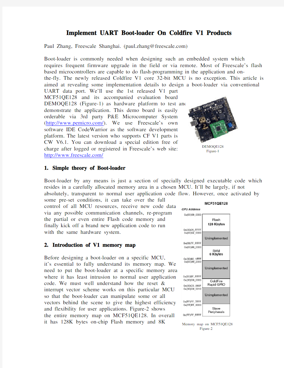
DEMOQE128 (Figure-1) as hardware platform to test and
demonstrate the application. This demo board is easily
orderable via 3rd party P&E Microcomputer System
(https://www.360docs.net/doc/c614042481.html,/). We use Freescale’s own
software IDE CodeWarrior as the software development
platform. The latest version who supports CF V1 parts is
CW V6.1. You can download a special edition free of charge after logged or registered in Freescale’s web site: https://www.360docs.net/doc/c614042481.html,/
1. Simple theory of Boot-loader
Boot-loader by any means is just a section of specially designed executable code which resides in a carefully allocated memory area in a chosen MCU. It’ll be largely, if not absolutely, transparent to normal user application code flow. However, once activated by
some pre-set conditions, it can take over the full
control of all MCU resources, receive new code data
via any possible communication channels, re-program
the partial or even entire Flash code memory and
finally kick off a brand new application code to run
with the same hardware system.
2. Introduction of V1 memory map
Before designing a boot-loader on a specific MCU,
it’s essential to fully understand its memory map. We
need to put the boot-loader at a specific memory area
where it has least intrusion to normal user application
code. We must well understand how the reset &
interrupt vector scheme works on this particular MCU
so that the boot-loader can manipulate some or all
vectors behind the scene to give the highest efficiency
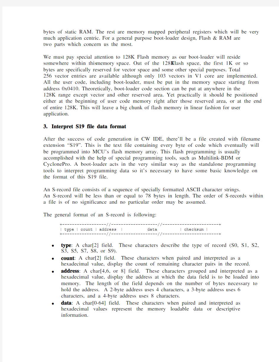
and flexibility for user applications. Figure-2 shows
the entire memory map on MCF51QE128. In overall it has 128K bytes on-chip Flash memory and 8K DEMOQE128 Figure-1 Memory map on MCF51QE128
Figure-2
bytes of static RAM. The rest are memory mapped peripheral registers which will be very much application centric. For a general purpose boot-loader design, Flash & RAM are two parts which concern us the most.
We must pay special attention to 128K Flash memory as our boot-loader will reside somewhere within this memory space. Out of the 128K Flash space, the first 1K or so bytes are specifically reserved for vector space and some other special purposes. Total 256 vector entries are available although only 103 vectors in V1 core are implemented. All the user code, including boot-loader, must be put in the memory space starting from address 0x0410. Theoretically, boot-loader code section can be put at anywhere in the 128K range except vector and other reserved area. Yet practically it should be positioned either at the beginning of user code memory right after those reserved area, or at the end of entire 128K. This will leave a big chunk of flash memory in linear fashion for user application.
3.Interpret S19 file data format
After the success of code generation in CW IDE, there’ll be a file created with filename extension “S19”. This is the text file containing every byte of code which eventually will be programmed into MCU’s flash memory array. This flash programming is usually accomplished with the help of special programming tools, such as Multilink-BDM or CyclonePro. A boot-loader acts in the very similar way as the standalone programming tools to interpret programming data so it’s necessary to have some basic knowledge on the format of this S19 file.
An S-record file consists of a sequence of specially formatted ASCII character strings. An S-record will be less than or equal to 78 bytes in length. The order of S-records within a file is of no significance and no particular order may be assumed.
The general format of an S-record is following:
+------------------//-------------------//-----------------------+
| type | count | address | data | checksum |
+------------------//-------------------//-----------------------+ ?type: A char[2] field. These characters describe the type of record (S0, S1, S2, S3, S5, S7, S8, or S9).
?count: A char[2] field. These characters when paired and interpreted as a hexadecimal value, display the count of remaining character pairs in the record.
?address: A char[4,6, or 8] field. These characters grouped and interpreted as a hexadecimal value, display the address at which the data field is to be loaded into memory. The length of the field depends on the number of bytes necessary to hold the address. A 2-byte address uses 4 characters, a 3-byte address uses 6 characters, and a 4-byte address uses 8 characters.
?data: A char[0-64] field. These characters when paired and interpreted as hexadecimal values represent the memory loadable data or descriptive information.
?checksum: A char[2] field. These characters when paired and interpreted as a hexadecimal value display the least significant byte of the ones complement of the sum of the byte values represented by the pairs of characters making up the count, the address, and the data fields.
Each record is terminated with a line feed. If any additional or different record terminator(s) or delay characters are needed during transmission to the target system it is the responsibility of the transmitting program to provide them.
S0 Record: The type of record is 'S0' (0x5330). The address field is unused and will be filled with zeros (0x0000). The header information within the data field is divided into the following subfields.
mname is char[20] and is the module name.
ver is char[2] and is the version number.
rev is char[2] and is the revision number.
description is char[0-36] and is a text comment.
Each of the subfields is composed of ASCII bytes whose associated characters, when paired, represent one byte hexadecimal values in the case of the version and revision numbers, or represent the hexadecimal values of the ASCII characters comprising the module name and description.
S1 Record: The type of record field is 'S1' (0x5331). The address field is interpreted as a 2-byte address. The data field is composed of memory loadable data.
S2 Record: The type of record field is 'S2' (0x5332). The address field is interpreted as a 3-byte address. The data field is composed of memory loadable data.
S3 Record: The type of record field is 'S3' (0x5333). The address field is interpreted as a 4-byte address. The data field is composed of memory loadable data.
S5 Record: The type of record field is 'S5' (0x5335). The address field is interpreted as a 2-byte value and contains the count of S1, S2, and S3 records previously transmitted. There is no data field.
S7 Record: The type of record field is 'S7' (0x5337). The address field contains the starting execution address and is interpreted as 4-byte address. There is no data field.
S8 Record: The type of record field is 'S8' (0x5338). The address field contains the starting execution address and is interpreted as 3-byte address. There is no data field.
S9 Record: The type of record field is 'S9' (0x5339). The address field contains the starting execution address and is interpreted as 2-byte address. There is no data field.
Coldfire V1 core is a 32-bit controller which naturally has 32-bit wide address. Therefore possible S-records could be S0, S3, S5, S7. And in practical, S0, S3 & S7 are three most often seen S-records in a S19 file for CF V1.
EXAMPLE:
Shown below is a typical S-record format file on CF V1 code.
S0030000FC
S321000024004E7551FC4E7551FC2F0E2F0CB1C9671C60102C48204E52882849224C1A
S70500002534A1
The S0 record is comprised as follows:
S0S-record type S0, indicating it is a header record.
03Hexadecimal 03 (decimal 3), indicating that three character pairs (or ASCII bytes) follow.
00 00 Four character 2-byte address field, zeroes in this example.
FC The checksum.
The S3 record is comprised as follows:
S3 S-record type S3, indicating it is a data record to be loaded at a 4-byte address.
21Hexadecimal 21 (decimal 33), indicating that thirty-three character pairs, representing a 4 byte address, 28 bytes of binary data, and a 1 byte checksum,
follow.
00 00 24 00 Eight character 4-byte address field; hexadecimal address 0x00002400,
where the data which follows is to be loaded.
4E 75 51 FC 4E 75 51 FC 2F 0E 2F 0C B1 C9 67 1C 60 10 2C 48 20 4E 52 88 28
49 22 4C twenty-eight character pairs representing the actual binary data.
1A The checksum.
The S7 record is comprised as follows:
S7 S-record type S7, indicating it is a termination record.
05 Hexadecimal 05 (decimal 5), indicating that five character pairs follow.
00 00 25 34The address field, hexadecimal 0x00002534 indicating the starting
execution address.
A1The checksum.
For a boot-loader in CF V1 MCU, the most important task is to receive S3-records, interpret each data section and program a string of payload data into flash memory starting from a specified address. S0-record is simply discarded because it contains no meaningful data for programming. S7-record tells the boot-loader it’s the end of S19 file and usually boot-loader will reboot the system with the updated firmware after acknowledge this line.
On PC or other type of data terminal who feeds the S19 data to MCU boot-loader, the data format could be in original ASCII text form as shown in above example. This will be the simplest approach but the download speed will be a bit slow as the S19 text file has lots of redundancy due to the nature of ASCII coding. The boot-loader at MCU side will handle all the data analysis and reformatting. One alternative is to analyze and reformat the S19 text line at PC side and streamline the payload data before sending to MCU boot-loader with user defined protocol. For the implementation in this article, we designed a simple PC software which read every S-record text line, appended with hex code 0x00 as
end-of-line tag, and then send this text string to 51QE128 boot-loader, which will do the rest of the job.
4.Memory segmentation for boot-loader design
Keep in mind that a boot-loader will be activated only when in need. It takes a block of permanent space in flash memory to reside and not a single byte of RAM is required while it’s inactive. When it’s in active mode, there’s no longer any user code running so it’s perfectly okay a boot-loader shares all RAM space with user application at different time. Therefore we only need to allocate proper flash memory space for a boot-loader.
A boot-loader has the capability to reprogram partial or entire flash memory subject to the actual application needs. Both approaches have their own advantages and disadvantages. To reprogram the entire flash, the boot-loader itself must firstly be copied into RAM and run its code from there in rest of the process. The advantage is obvious – it can erase and reprogram the entire code space at your own wishes. The disadvantage is the high risk of reprogramming process abortion because of power-down or any kind of unexpected chip resets. This will leave the code space blank or partially programmed and there’s no way to bring it back except to reprogram the chip with standalone programmer.
A more reliable and safer way is to put the boot-loader code section into a permanent area where it’ll never be erased by boot-loader itself. The goal is to be able to get boot-loader up and running even after all the user application codes are erased, or only partially programmed. To achieve this, boot-loader must be the first part to run after any reset – i.e. the reset vector entry must point to the boot-loader, not user code. Since the boot-loader is fixed in flash memory, the whole vector table MUST also be fixed because a smallest flash page to be erased and reprogrammed is 1024-byte size in V1 core. This again leads to the topic of the redirection of vector entries in user code.
Redirection of vector entry is achieved by setting the original vector table (0x000-0x3FFF) with fixed index entry (address) of another user defined table. The original table will permanently reside in flash memory as same as boot-loader section. The user defined new table will have every entry offset address fixed but the contents in that entry are free to change, usually its content in each entry is a simple “jmp” instruction to jump the code to real vector service routine, which will be either initialization code after reset or any kinds of interrupt service routine. Figure-3 illustrated this kind of approach.
As such, we divided the 128K flash memory into 4 segments: 1K or so bytes of original vector table (with a few bytes of reserved space); 2K bytes of boot-loader code, which can be more or less depends on actual code size requirement; 1K bytes of user defined redirected vector table; the rest are for user applications. The first two segments are fixed in permanent once programmed with standalone programmer, the rest are all user reprogrammable by boot-loader for highest application flexibility. Figure-4 shows the flash memory map under this arrangement.
5. Implementation of boot-loader
Now let’s get into the real design work of an UART based boot-loader on MCF51QE128. As mentioned earlier, we use DEMOQE128 board as the hardware platform so it’s necessary to check with the board schematic for better understanding of any hardware related control or setup in the below demo code.
5.1
Modification of project linker command file (lcf file) When we use CW project wizard to create a new
project, there’ll be a project linker command file
(lcf as its extension filename, see example in
Figure-5) created automatically, which defines the
allocation and usage of all available ROM (flash) &
RAM resources associated with the selected chip.
We must manually alter parts of its contents so as to
get the memory segmentation as per the description
in chapter 4. In this file there is an important text block called MEMORY {} which consists of all the definitions for different memory segments. A
default lcf file for 51QE128 may have memory
definitions look like this:
MEMORY {
code (RX) : ORIGIN = 0x00000410, LENGTH = 0x0001FBF0
Project lcf file Figure - 5
userram (RWX) : ORIGIN = 0x00800000, LENGTH = 0x00002000
}
It simply declares two memory segments, one is for code area (flash ROM) with starting address at 0x00000410 and length of 0x0001FBF0; the other one is for RAM area with starting address at 0x00800000 and length of 0x00002000. Note there’s no need to explicitly declare system vector area as the address range 0x00000000-0x0000040F is already reserved by linker for this purpose.
Now we need to modify this memory declaration to accommodate boot-loader memory segmentation requirement as below.
MEMORY {
userram (RWX) : ORIGIN = 0x00800000, LENGTH = 0x00002000
BootLoad (RX) : ORIGIN = 0x00000410, LENGTH = 0x000007F0
VectorReMap (RX) : ORIGIN = 0x00000C00, LENGTH = 0x00000400
code (RX) : ORIGIN = 0x00001000, LENGTH = 0x0001F000
}
So we divided the flash ROM into 3 segments: 2K bytes (0x00000410-0x00000BFF) specifically for boot-loader; 1K bytes (0x00000C00-0x00000FFF) for vector redirection; and the rest area (0x00001000-0x0001EFFF) are free for user application code.
Next, we need to add something in the middle of another text block called SECTIONS {}. We can leave all the existing contents untouched but add in following lines
# define code sections
.BootLoad : {} > BootLoad
.VectorReMap : {} > VectorReMap
# Code placement for boot-loader section
.text_bootload :
{
BootLoad.c (.text_bootload)
. = ALIGN (0x4);
} >> BootLoad
# Code placement for remapped vector section
.text_vectormap :
{
VectorMap.c (.text_vectormap)
. = ALIGN (0x4);
} >> VectorReMap
The above statement tells the linker where to put boot-loader code segment (declared as “text_bootload” in source file) and vector redirection segment (declared as “text_vectormap” in source file). The key message here is: once we modified this lcf file for boot-loader design, it must be used for user application design in the exactly same form.
5.2Coding of Boot-Loader
Most of the boot-loader coding works are as same as for normal applications, except you must be able to tell the linker that all the codes belong to boot-loader will be eventually put in a special section as stated in lcf file for permanent residence in flash memory. We use “#pragma” to declare a unique code section for this purpose:
//=============================================================================
// Declare a code segment with name "text_bootload"
//=============================================================================
#pragma CODE_SEG __FAR_SEG text_bootload
Note the highlighted section name must match with the reference in lcf file showing in above sect 5.1
5.2.1Create reset vector and its service routine
We shall also tell the complier and linker that boot-loader must be the first part to run after any kinds of reset. We can declare a reset-vector function by doing below:
//=============================================================================
// - Vector 1 - Reset vector
//
// - This portion of code will be executed right after reset.
// - The purpose is to check if it should go to normal code flow or get into
// Boot-loader by checking key-press on PortD pin3 and validity of vector area
//=============================================================================
void interrupt VectorNumber_INITPC FirstHandChk(void)
{
…
}
The keyword “interrupt” tells the complier this is a vector type of function although it’s not a real interrupt for this reset vector. “VectorNumber_INITPC” is pre-defined in project header file MCF51QE128.h as the vector number for MCU reset. By declaring a function in this form, the reset vector in the original vector table will point to this function after code generation.
There are four major parts in this function:
1.Setup key registers A7, A6 & A5 for basic code running environment. A7 is the stack
pointer; A6 is the stack frame register; A5 is used for RAM relative-addressing, if so required;
//setup A7 stack pointer
asm (lea _SP_INIT, a7);
//setup A6 dummy stackframe
asm (movea.l #0, a6);
asm (link a6, #0);
//setup A5
asm (lea _SDA_BASE, a5);
2.Check the hardware key-pressing (associated with eval board hardware). It’ll activate
boot-loader unconditionally if a key-pressing on PortD pin3 is confirmed;
//setup PORTD3 for key-press detection
PTDDD_PTDDD3 = 0; //set PTD3 as input (key)
// check if boot-loader function is activated by pressing PortD pin3
// upon reset
if (!PTDD_PTDD3) { //pin is low - possible key-press detected
for (wTmp=0;wTmp<1024;wTmp++) {} //delay for key debouncing
if (!PTDD_PTDD3) { //double-check to confirm key-press
asm (jmp BootLoader); //Boot-loader activation confirmed, jump to //Boot-loader routine
}
}
3.Or check the validity of user application code contents by simply verifying the
leading 16 bytes of programmed data in new redirected vector table. User can design
a more reliable way which is to calculate the checksum of entire reprogrammable
memory space.
//Boot-loader is not activated by key upon reset,
//Need to further verify if normal code flow exists
//by checking 1st 16 bytes of data in remapped vector area
datPtr = (void*)StartupEntry; //get the starting address by referring to 1st
//entry in redirected vector map
for (bTmp=0;bTmp<16;bTmp++) { //check for consecutive 16 bytes
if (*(byte*)datPtr != 0xff) //break out if any one is not 0xff
break;
((byte*)datPtr)++;
}
if (bTmp==16) { //leading 16 bytes in vector map are all 0xff,
//vector map is invalid
asm (jmp BootLoader); //Jump to Boot-loader routine
}
4.Execute the normal user application code flow if neither special key-pressing is found
upon reset, nor is user code invalid.
//execute normal code follow
asm (jmp StartupEntry); //Jump to normal "startup" routine
5.2.2Boot-loader main working loop
The main boot-loader function also consists of four portions.
//=============================================================================
// Boot-loader main routine
//=============================================================================
void BootLoader(void)
{
…
}
1.Setup key registers A7, A6 & A5 as same as what it does in reset vector routine. This
is because it is possible a boot-loader will be evoked by user code flow after matching with pre-set condition, for example a special command from normal UART communication.
2.Disable all interrupt and do some initialization works. There is no any kind of
interrupt allowed during boot-loader process because the redirected vector table will be erased for new updates. The key initialization works are system clock module and SCI module setup in this example.
DisableInterrupts; //disable all interrupt, no interrupt is allowed
//Do all the initialization works
InitBootLoad();
3.Copy a key portion of flash programming code into RAM buffer for real
programming usage. This is because the code execution running in flash will not be reliable if the flash itself is undergoing erase/programming. Then we do erase for all the user reprogrammable flash space.
//Copy flash-command execution code into RAM
CopyRom2Ram((byte*)FlashCmdExec, 128);
//Erase all pages in reprogrammable area
FlashErase();
4.Execute a dead loop for polling two things – receive S19 text line for new code
download and programming, and check the timer overflow to toggle LEDs as simple user interface signaling.
//Boot-loader main loop
for (;;) {
__RESET_WATCHDOG(); //clear watchdog
ReceiveS19Text(); //polling to process incoming data
TPM1OverflowChk(); //polling to check timer
}
5.2.3Receive S19 line and flash programming
Receiving of S19 text lines are driven by a state-machine showing in below Figure-6. It’ll receive every S19 line and echo back with an ASCII code “.” as acknowledgment. It interprets each S3 line and program the data into designated flash memory. It can automatically reboot the system by deliberately jumping the code to an illegal address once an S7 line is received and acknowledged.
Please refer to project source code for details within function of
void ReceiveS19Text(void){
...
}
5.3Vector redirection
Redirection of original vector table is accomplished by defining a specific code segment where we implement all the interrupt service entry for every possible interrupt source. Yet there is actually no meaningful code in each entry except a simple instruction of code jump to a real service routine implemented in user application. There’s no such need to follow the exact ascending order of natural vector number for this remapping. But once
defined and fixed, the order and size of each service entry MUST NOT be changed in user application. This is because the contents in the original vector table will be filled up with the mapped address when complier and linker generate this boot-loader code, and it’s not alterable again by boot-loader itself once programmed into the flash. For all those unused vector entries we can set a default trap for address redirection so as to keep the code size unchanged even if they’ll be utilized later on. Remember we also need to put this redirected vector table at an address specified in lcf file:
#pragma CODE_SEG __FAR_SEG text_vectormap
Each vector redirection can be written as following in default:
//=============================================================================
// Entry of normal code flow
//=============================================================================
void StartupEntry(void)
{
asm (jmp _startup);
}
void interrupt VectorNumber_Vaccerr ISR_Vaccerr(void)
{
asm (jmp IllegalTrap);
}
void interrupt VectorNumber_Vadderr ISR_Vadderr(void)
{
asm (jmp IllegalTrap);
}
...
void interrupt VectorNumber_VL1swi ISR_VL1swi(void)
{
asm (jmp IllegalTrap);
}
//=============================================================================
// Setup a trap for unexpected interrupt request
//=============================================================================
void IllegalTrap(void)
{
while(1){
;
}
}
Take note the first entry named as “StartupEntry”, which is not an interrupt-type of function. This is because we’ve already set the reset vector in boot-loader segment and this is just a fixed entry to redirect to normal startup code section under standard C programming.
The last piece of vector remap is a simple trap for illegal vector interception, which also acts as a default vector service contents for a boot-loader design.
5.4Dummy main() function in boot-loader design
As we go through standard application development procedure for a special boot-loader design, a dummy main() function is needed to eliminate final linker error. This function is as simple as below:
void BootLoader(void);
#pragma CODE_SEG __FAR_SEG DEFAULT
//=============================================================================
//=============================================================================
void main(void) {
asm (jmp BootLoader); //Jump to Boot-loader routine
}
It simply jumps to the main boot-loader code section, if it ever gets opportunity to run. 5.5Program boot-loader code into flash
Once the boot-loader is coded, complied and linked successful, we can use standalone programmer tools such as MultiLink-BDM or CyclonePro to program the machine code into QE128 flash memory. After removing the programming tools and having a power-up reset, the boot-loader will be running with PTC0 LED flickering at a fast pace on QE128 demo board, indicating it’s in boot-loader mode and ready to receive new firmware via UART port.
6.Coding of user application
Coding of user code is nothing too special, but with some key points in mind:
?Use the same lcf file as for boot-loader project to keep the exact same flash memory segmentation;
?Add module “VectorMap.c” into application project with its file name intact as lcf will filter out “.text_vectormap” section only from this file;
?Within “VectorMap.c”, do not insert or delete the function entry in vector remap segment. Only modify the destination address in “jmp” instruction for redirection of specific interrupt service routine.
The only point worth to elaborate a bit more is the implementation of user specified interrupt service routine. In user code we implement an interrupt service routine simply by assigning a key word “interrupt” in front of function name as below example. There’s no need to assign associated vector number, although it might cause a warning message during compiling, just ignore it.
//=============================================================================
// - User application SCI1 data receive interrupt service routine
// - Must update ISR_Vsci1rx in 'VectorMap.c' for proper re-direction as this:
// asm (jmp App_SCI1Rx_ISR);
//=============================================================================
void interrupt App_SCI1Rx_ISR(void)
{
byte dat;
SCI1S1; //read the status register once to clear RDRF bit
dat = SCI1D; //read the data in SCI buffer, RDRF bit is cleared now
SCI1D = dat; //echo back in test mode
}
In order to get this ISR running as expected, we must modify the code-jump instruction in remapped vector table as below:
//declare function prototype
void App_SCI1Rx_ISR(void);
...
// *** SCI1 RX ISR Utilized
void interrupt VectorNumber_Vsci1rx ISR_Vsci1rx(void)
{
//asm (jmp IllegalTrap); //default entry
asm (jmp App_SCI1Rx_ISR); //user ISR entry
}
Please follow the above example for all user defined ISR redirection – declare user ISR function prototype on top of the code lines firstly and modify the related “jmp” instruction for ISR redirection.
7.PC download software
A simple PC software is developed to test and implement the 51QE128 boot-loader design discussed above. It has three operations: setup the PC UART port to 38400-N-8-1; open an S19 file to download; and download the selected S19 file contents to target board.
8.Project source code and demonstration
Complete reference source code for boot-loader and sample user applications are available. Executable PC side download software is also provided for demo purpose. All the source code are subject to “as is” agreement. Users are free to change the code and take own risk.
To run the demo code, we must firstly program the boot-loader code (BootLoader.S19) into MCU using standalone programmer. The demo board will be running in boot-loader mode if this programming is successful. Connect QE128 demo board and PC with a null-modem RS232 cable, run PC download software and down load a sample application
(DemoApp1.S19) to target board. The new application will start to run automatically after download.
To activate boot-loader again, please hold-down PTD3 key and perform any kind of reset, the board will enter boot-loader and be ready to receive new firmware via UART port. References:
MCF51QE128 reference manual
ColdFireV1 build tools reference
飞思卡尔单片机编程
关于Codewarrior 中的 .prm 文件 网上广泛流传的一篇文章讲述的是8位飞思卡尔单片机的内存映射,这几天,研究了一下Codewarrior 5.0 prm文件,基于16位单片机MC9S12XS128,一点心得,和大家分享。有什么错误请指正。 正文: 关于Codewarrior 中的.prm 文件 要讨论单片机的地址映射,就必须要接触.prm文件,本篇的讨论基于Codewarrior 5.0 编译器,单片机采用MC9S12XS128。 通过项目模板建立的新项目中都有一个名字为“project.prm”的文件,位于Project Settings->Linker Files文件夹下。一个标准的基于XS128的.prm文件起始内容如下: .prm文件范例: NAMES END SEGMENTS RAM = READ_WRITE DATA_NEAR 0x2000 TO 0x3FFF;
READ_ONLY DATA_NEAR IBCC_NEAR 0x4000 TO 0x7FFF; ROM_C000 = READ_ONLY DATA_NEAR IBCC_NEAR 0xC000 TO 0xFEFF; //OSVECTORS = READ_ONLY 0xFF10 TO 0xFFFF; EEPROM_00 = READ_ONLY DATA_FAR IBCC_FAR 0x000800 TO 0x000BFF; EEPROM_01 = READ_ONLY DATA_FAR IBCC_FAR 0x010800 TO 0x010BFF; EEPROM_02 = READ_ONLY DATA_FAR IBCC_FAR 0x020800 TO 0x020BFF; EEPROM_03 = READ_ONLY DATA_FAR IBCC_FAR 0x030800 TO 0x030BFF; EEPROM_04 = READ_ONLY DATA_FAR IBCC_FAR 0x040800 TO 0x040BFF; EEPROM_05 = READ_ONLY DATA_FAR IBCC_FAR 0x050800 TO 0x050BFF; EEPROM_06 = READ_ONLY DATA_FAR IBCC_FAR 0x060800 TO 0x060BFF; EEPROM_07 = READ_ONLY DATA_FAR IBCC_FAR 0x070800 TO 0x070BFF; PAGE_F8 = READ_ONLY DATA_FAR IBCC_FAR 0xF88000 TO 0xF8BFFF;
飞思卡尔锁相环
备战飞思卡尔智能车大赛.开始模块总结. 锁相环设置. 公式: PLLCLK=2*OSCCLK*(SYNR+1)/(REFDV+1), fbus=PLLCLK/2 void INIT_PLL(void) { CLKSEL &= 0x7f; //选用外部时钟.准备设置锁相环 PLLCTL &= 0x8F; //禁止锁相环 SYNR = 0xc9; //设置SYNR REFDV = 0x81; //设置REFDV PLLCTL |=0x70; //锁相环使能 asm NOP; asm NOP; //两个机器周期缓冲时间 while(!(CRGFLG&0x08)); //等待锁相环锁定 CLKSEL |= 0x80; //设置锁相环为时钟源 } 飞思卡尔XS128的PLL锁相环详细设置说明——关于如何提高总线工作频率PLL锁相环就相当于超频 单片机超频的原因和PC机是个一道理。分频的主要原因是外设需要的工作频率往往远低于CPU/MEMORY 这也和PC机南北桥的原理类似。总线频率设置过程 1、禁止总中断 2、寄存器CLKSEL(时钟选择寄存器)的第七位置0 即CLKSEL_PLLSEL=0。选择时钟源为外部晶振OSCCLK(外接晶振频率) 在PLL(锁相环)程序执行前 内部总线频率为OSCCLK/2 3. PLLCTL_PLLON=1 打开PLL 4.设置SYNR 时钟合成寄存器 、REFDV 时钟分频寄存器 、POSTDIV三个寄存器的参数 5、_asm(nop) _asm(nop);加入两条空指令 使锁相环稳定 6、while(!(CRGFLG_LOCK==1));//时钟校正同步 7、CLKSEL_PLLSEL=1; 下面详细说一下频率的计算一、时钟合成寄存器SYNR寄存器结构 VCOFRQ[1:0]控制压控振动器VCO的增益 默认值为00 VCO的频率与VCOFRQ[1:0]对应表
飞思卡尔智能车比赛细则
2016
目录
第十一届竞赛规则导读 参加过往届比赛的队员可以通过下面内容了解第十一届规则主要变化。如果第一次参加比赛,则建议对于本文进行全文阅读。 相对于前几届比赛规则,本届的规则主要变化包括有以下内容: 1.本届比赛新增了比赛组别,详细请参见正文中的图1和第四章的“比赛任务” 中的描述; 2.第十届电磁双车组对应今年的A1组:双车追逐组。其它组别与新组别的对应 关系请参见图2; 3.为了提高车模出界判罚的客观性,规则提出了两种方法:路肩法和感应铁丝 法,详细请见赛道边界判定”; 4.改变了原有的光电计时系统,所有赛题组均采用磁感应方法计时,详细请参 见“计时裁判系统”; 5.取消了第十届的发车灯塔控制的方式; 6.赛道元素进行了简化,详细请参见“赛道元素”; 7.赛道材质仍然为PVC耐磨塑胶地板,但赛题组A2不再需要赛道。 8.对于车模所使用的飞思卡尔公司MCU的种类、数量不再限制。 9.比赛时,每支参赛队伍的赛前准备时间仍然为20分钟,没有现场修车环节。
一、前言 智能车竞赛是从2006开始,由教育部高等教育司委托高等学校自动化类教学指导委员会举办的旨在加强学生实践、创新能力和培养团队精神的一项创意性科技竞赛。至今已经成功举办了十届。在继承和总结前十届比赛实践的基础上,竞赛组委会努力拓展新的竞赛内涵,设计新的竞赛内容,创造新的比赛模式,使得围绕该比赛所产生的竞赛生态环境得到进一步的发展。 为了实现竞赛的“立足培养、重在参与、鼓励探索、追求卓越”的指导思想,竞赛内容设置需要能够面向大学本科阶段的学生和教学内容,同时又能够兼顾当今时代科技发展的新趋势。 第十一届比赛的题目在沿用原来根据车模识别赛道传感器种类进行划分的基础类组别之上,同时增加了以竞赛内容进行划分的提高类组别,并按照“分赛区普及,全国总决赛提高”的方式,将其中一个类别拓展出创意类组别。第十一届比赛的题目各组别分别如下: ●基础类包括B1光电组、B2摄像头组、B3电磁直立组、B4电轨组; ●提高类包括A1双车追逐组、A2信标越野组; ●创意类包括I1 电轨节能组。 图 1 不同组别,不同挑战度 每个组别在选用的车模、赛道识别方法、完成任务等方面存在差别,对于参赛选手不同学科知识和能力要求也不同,制作的挑战度也有较大的区别。相比较而言,
飞思卡尔单片机LED控制例程详解
我的第一个LED程序 准备工作: 硬件:Freescale MC9S08JM60型单片机一块; 软件:集成开发环境codewarrior IDE; 开发板上有两个LED灯,如下图所示: 实验步骤: 1.首先,确保单片机集成开发环境及USBDM驱动正确安装。其中USBDM的安装步骤如下:?假设之前安装过单片机的集成开发环境6.3版本:CW_MCU_V6_3_SE; ?运行USBDM_4_7_0i_Win,这个程序会在c盘的程序文件夹下增加一个目录C:\Program Files\pgo\USBDM 4.7.0,在这个目录下: 1〉C:\ProgramFiles\pgo\USBDM 4.7.0\FlashImages\JMxx下的文件 USBDM_JMxxCLD_V4.sx是下载器的固件文件; 2〉C:\Program Files\pgo\USBDM 4.7.0\USBDM_Drivers\Drivers下有下载器的usb 驱动 所以在插入usb下载器,电脑提示发现新的usb硬件的时候,选择手动指定驱动 安装位置到以上目录即可。 ?运行USBDM_4_7_0i_Win之后,还会在目录: C:\Program Files\Freescale\CodeWarrior for Microcontrollers V6.3\prog\gdi 下增加一些文件,从修改时间上来看,增加了6个文件,这些文件是为了在codewarrior 集成开发环境下对usb下载器的调试、下载的支持。
2.新建一个工程,工程建立过程如下: ?运行单片机集成开发环境codewarrior IDE ?出现如下界面 ●Create New Project :创建一个新项目工程 ●Load Example Project :加载一个示例工程 ●Load Previous Project :加载以前创建过的工程 ●Run Getting started Tutorial:运行CodeWarrior软件帮助文档 ●Start Using CodeWarrior:立刻使用CodeWarrior ?点击Create New project按钮,以创建一个新的工程,出现选择CPU的界面 如下,请选择HCS08/HCS08JM Family/MC9S08JM60,在右边的Connection窗口
飞思卡尔智能车竞赛新手入门建议
每年都会有很多新人怀着满腔热情来做智能车,但其中的很多人很快就被耗光了热情和耐心而放弃。很多新人都不知道如何入手,总有些有劲无处使的感觉,觉得自己什么都不会,却又不知道该干什么。新人中存在的主要问题我总结了以下几点: l缺乏自信,有畏难情绪 作为新人,一切都是新的。没有设计过电路,没有接触过单片机,几乎什么都不会。有些新人听了两次课,看了两篇技术报告,就发现无数不懂不会的东西,于是热情在消退,信心在减弱。这些都是放弃的前兆。殊不知,高手都是从新人过来的,没有谁天生什么都会做。一件事件,如果还没开始做,就自己否定自己,认为自己做不到,那么肯定是做不到的。 l习惯了被动接收知识,丧失了主动学习的能力。 现在的学生大多从小习惯了被灌输知识,只学老师教的,只学老师考的。殊不知一旦走向社会,将不再有老师来教,不再有应付不完的考试。做智能车和传统的教学不同,学生将从被动学习的地位转变为主动学习。就算有指导老师,有指导的学长,但也都处于被动地位,往往都不会主动来教。有的学生一开始就没有转变思想,还希望就像实验课一样,老师安排好步骤1,2,3……,然后自己按照老师安排好的步骤按部就班的完成。这样的学生,往往都丧失了提出问题和分析问题的能力,只是一个应付考试的机器。要知道,解决问题的第一步是提出问题,如果总等着别人来教,那么问题永远会挡在你面前。 l缺乏团队精神和合作意识 智能车比赛是以团队的形式参赛,只依靠个人能力单兵作战就能取得好成绩的是很少很少的。当今社会,任何人的成功都离不开身后的团队的支撑。智能车是一个很复杂的系统,电路、机械、传感器、单片机、底层驱动、控制算法……。如果所有的任务都是一个人去完成,固然锻炼了自己,但想做的很好却很不现实。很多新人,来到实验室,来到一个陌生的环境和团队,连向学长请教,和同学交流的勇气都没有,又如何融入团队呢。除了要主动融入团队,还要培养自己的团队意识。团队精神往往表现为一种责任感,如果团队遇到问题,每个人都只顾自己,出了错误,不想着解决问题,而是互相推诿埋怨。这样的团队,肯定是无法取得好成绩的。 l缺乏耐心和细心的精神 其实把一件事做好很简单,细心加上耐心。不细心就想不到,没有耐心,即使想到了也做不到。做事怕麻烦,将就,说白了就是惰性在作祟。明明可以把支架做的更轻更漂亮,明明可以把程序写的更简洁,明明可以把电路设计得更完善……。其实,每个人都有很大潜力,如果不逼自己一次,你永远不知道自己的潜力有多
飞思卡尔单片机知识点
1、单片机组成:1> CPU 2> 存储器3>I/O ; 2、存储器包括2大类:ROM , RAM 3、标准ASCII码使用(1)个字节表示字符; 4、BCD码是用()进制表示的()的数据; 5、HCS08QG8的最小系统包括(电源电路,复位电路,下载口,(内部时钟)); 6、QG8管脚数量(16)、只能输入的是(PTA5)、只能输出的是(PTA4)、程序下载的是、接外部时钟的是; 7、QG8的管脚可以作为数字输入输出、也可以作为模拟输入,可以作为模拟输入的有(); 8、QG8管脚复用优先级最低的功能是(I/O); 9、QG8存储器配置中,不同资源的分界线……; 10、CPU寄存器有(A, HX, PC, CCR, SP); 11、可以执行位操作的地址范围(0X0000~0X005F); 12、有地址的寄存器分成了(3)块(0页,高页,非易失); 13、如何在C语言中定义常数(数据类型变量名;),如何指定变量的地址(数据类型变量名@ 地址;); 14、堆栈的管理者是寄存器(SP); 15、SP的复位缺省值是(0X00FF); 16、堆栈对数据的操作特点是(向上生长型:先压后涨、先减后弹); 17、堆栈一般在RAM的高地址区域还是低地址区域?高地址区 18、内部时钟源包括哪4大部分? 19、外部时钟分哪2大类;振荡器,整形外部时钟 20、内部时钟中FLL固定倍频(512倍频); 21、ICS的7种工作模式(FEI, FEE, FBI, FBILP, FBE, FBELP, stop); 22、ICS的内部参考时钟是可以校准、微调的,调整的寄存器名(ICSTRM);该寄存器的数值越大,输出时钟频率越(低); 23、FLASH是按页管理的,页大小(512)字节,每页分(8)行; 24、高页寄存器位于FLASH的最后一页的(第六行/0xFFB0~0xFFBF)位置; 25、FLASH的最后一页最后一行是(中断向量); 26、FLASH块保护寄存器(FPROT);块加密寄存器(FOPT);对应的非易失寄存器分别是(NVOPT, NVPROT); 27、FLASH操作的一般过程是(); 28、FLASH操作的有效命令有(空检查,字节编程,突发模式编程,页擦除,全部ROM 擦除); 29、记录程序运行状态的CPU寄存器是(CCR); 30、指令系统包括6大类指令,分别是(算术运算指令、数据传送指令、数据和位操作、逻辑运算、程序控制、堆栈处理); 31、寻址方式是指(CPU访问操作数和数据的方法); 32、寻址方式包括7大类16种,分别是: INH IMM DTR EXT IX,IX1,IX2,SP1,SP2,IX+,IX1+ REL IMD, DD,IX+D,DIX+ 33、8指令模板和6指令模板分别是(); 34、QG8是高电平复位还是低电平复位?低电平 35、QG8数据存储器RAM的大小为(512)字节; 36、上电复位期间将管脚(A4)设置为(低)电平可以进入调试模式 37、QG8的存储器结构为冯·诺伊曼还是哈佛结构?冯诺依曼
飞思卡尔杯智能车竞赛报告总结
1.1. 系统分析 智能车竞赛要求设计一辆以组委会提供车模为主体的可以自主寻线的模型车,最后成绩取决于单圈最快时间。因此智能车主要由三大系统组成:检测系统,控制系统,执行系统。其中检测系统用于检测道路信息及小车的运行状况。控制系统采用大赛组委会提供的16位单片机MC9S12XS128作为主控芯片,根据检测系统反馈的信息新局决定各控制量——速度与转角,执行系统根据单片机的命令控制舵机的转角和直流电机的转速。整体的流程如图1.1,检测系统采集路径信息,经过控制决策系统分析和判断,由执行系统控制直流电机给出合适的转速,同时控制舵机给出合适的转角,从而控制智能车稳定、快速地行驶。 图2.1 1.2. 系统设计 参赛小车将电感采集到的电压信号,经滤波,整流后输入到XS128单片机,用光电编码器获得实时车速,反馈到单片机,实现完全闭环控制。速度电机采用模糊控制,舵机采用PD控制,具体的参数由多次调试中获得。考滤到小车设计的综合性很强,涵盖了控制、传感、电子、电气、计算机和机械等多个学科领域,因此我们采用了模块化设计方法,小车的系统框图如图2.2。
第五届全国大学生智能汽车竞赛技术报告 图2.2 1.3. 整车外观 图2.3
1.4. 赛车的基本参数 智能车竞赛所使用的车模是东莞市博思公司生产的G768型车模,由大赛组委会统一提供,是一款带有摩擦式差速器后轮驱动的电动模型车。车模外观如图3.1。车模基本参数如表3.1。 图3.1 表3.1车模基本参数 1.5. 赛车前轮定位参数的选定
第五届全国大学生智能汽车竞赛技术报告 现代汽车在正常行驶过程中,为了使汽车直线行驶稳定,转向轻便,转向后能自动回正,减少轮胎和转向系零件的磨损等,在转向轮、转向节和前轴之间须形成一定的相对安装位置,叫车轮定位,其主要的参数有:主销后倾、主销内倾、车轮外倾和前束。模型车的前轮定位参数都允许作适当调整,故此我们将自身专业课所学的理论知识与实际调车中的赛车状况相结合,最终得出赛车匹配后的前轮参数[6]。 1.5.1. 主销后倾角 主销后倾角是指在纵向平面内主销轴线与地面垂直线之间的夹角γ,如图3-2。模型车的主销后倾角可以设置为0、 2°?3°、 4°?6°,可以通过改变上横臂轴上的黄色垫片来调整,一共有四个垫片,前二后二时为0°,前一后三为2°?3°,四个全装后面时为4°?6°。 由于主销后倾角过大时会引起转向沉重,又因为比赛所用舵机特性偏软,所以不宜采用大的主销后倾角,以接近0°为好,即垫片宜安装采用前二后二的方式,以便增加其转向的灵活性。如图3.3。 图3.2 图3.3 1.5. 2. 主销内倾角 主销内倾角是指在横向平面内主销轴线与地面垂直线之间的夹角β,如图3.4,它的作用也是使前轮自动回正。对于模型车,通过调整前桥的螺杆的长度可以改变主销内倾角的大小,由于前轴与主销近似垂直的关系,故主销内倾角
飞思卡尔第一张
3.1 实验一 I/O口输入输出实验 4.实验原理 如图3-1所示,将PTB6设置为输出端口后,若向PTB6写高电平时,LED灯不亮,若写低电平,则LED亮。PTA2设置为输入端口后,在按键SW未按下时,读PTA2始终为高电平,只有在按键SW按下时,读PTA2时才得到低电平。 图3-1 LED灯与按键控制电路原理图 5.实验内容 ⑴结合开发板电路图,用跳线夹连接对应LED引脚。即LED1、LED2分别与PTB6、PTB7相连接。将PTB 口定义为输出接口。对端口写0即可点亮LED灯。单步运行观察实验现象。 ⑵结合开发板电路图,用跳线夹再将开发板上的按键SW1、SW2连到PTA2。将PTA口定义为输入口,将PTB口定义为输出口。按下SW1时点亮LED1、LED2。按下SW2时熄灭LED1、LED2。 6.参考程序 ⑴直接点亮LED灯,其参考程序如下。 C语言程序: #include
for(;;) { __RESET_WATCHDOG(); /* 清看门狗 */ } /* 死循环 */ } 汇编程序(加粗部分为所需添加的程序代码): ;******************************************************************* ;* This stationery serves as the framework for a user application. * ;* For a more comprehensive program that demonstrates the more * ;* advanced functionality of this processor, please see the * ;* demonstration applications, located in the examples * ;* subdirectory of the "Freescale CodeWarrior for HC08" program * ;* directory. * ;******************************************************************* ; Include derivative-specific definitions INCLUDE 'derivative.inc' ; ; export symbols ; XDEF _Startup ABSENTRY _Startup ; ; variable/data section ; ORG RAMStart ; Insert your data definition here ExampleVar: DS.B 1 ; ; code section ; ORG ROMStart _Startup: LDHX #RAMEnd+1 ; initialize the stack pointer TXS CLI ; enable interrupts mainLoop: ; Insert your code here MOV #$FF,PTBDD; 端口方向寄存器初始化为输出 MOV #$FF,PTBD; 输出高点平,LED灯灭 MOV #$00,PTBD; 输出低电平,LED灯亮 NOP
飞思卡尔单片机优点
常有人问freescale的单片机有什么优点,今天转篇别人写的文章来,可以部分回答这些朋友的问题,但需要说明的是下面这篇文章主要是针对S08,S12这类单片机说的,飞思卡尔处理器远非只是单片机。飞思卡尔(freescale)半导体公司,就是原来的Motorola公司半导体产品部。于2004年从Motorola分离出来,更名为freescale!freescale系列单片机采用哈佛结构和流水线指令结构,在许多领域内都表现出低成本,高性能的的特点,它的体系结构为产品的开发节省了大量时间。此外freescale提供了多种集成模块和总线接口,可以在不同的系统中更灵活的发挥作用!所有单片机都具有的功能我就不多说了,freescale单片机的特有的特点如下: (1)全系列: 从低端到高端,从8位到32位全系列应有尽有,最近还新推出8位/32位管脚兼容的QE128,可以从8位直接移植到32位,弥补单片机业界8/32 位兼容架构中缺失的一环! (2)多种系统时钟模块:三种模块,七种工作模式 多种时钟源输入选项,不同的mcu具有不同的时钟产生机制,可以是RC振荡器,外部时钟或晶振,也可以是内部时钟,多数CPU同时具有上述三种模块!可以运行在FEI,FEE,FBI,FBILP,FBE,FBELP,STOP这七种工作模式! (3)多种通讯模块接口: 与其它系列的单片机不同,freescale单片机几乎在内部集成各种通信接口模块:包括串行通信接口模块SCI,多主I2C总线模块,串行外围接口模块SPI,MSCAN08控制器模块,通用串行总线模块(USB/PS2)! (4)具有更多的可选模块:某些MCU具有LCD驱动模块,某些MCU带有温度传感器,某些MCU具有超高频发送模块,部分MCu含有同步处理器模块,某写含有同步处理器的MCU 还具有屏幕显示模块OSD,还有少数的MCU具有响铃检测模块RING和双音多频/音调发生器DMG模块! (5)可靠性高,抗干扰性强 (6)低功耗 也许freescale系列的单片机的功耗没有msp430的低,但是他具有全静态的“等待”和“停止”两种模式,从总体上降低您的功耗!新近推出的几款超低功耗已经与msp430的不相上下! (7)多种引脚数和封装选择 可以说freescale系列单片机具有的MCU种类是最多的了,有些MCU本身就有几种不同的引脚数和封装形式,这样用户各异根据需要来选择,总有一款适合你的开发的单片机! 有关于部分人的freescale单片机模块寄存器多,配置困难不容易上手,可以说freescale单片机模块寄存器的确相对多,就拿GPIO来说就有端口数据寄存器、端口数据方向寄存器、端口内部上拉使能寄存器、端口转换率使能寄存器和端口驱动强度选择寄存器5个寄存器,它的寄存器多是为了解决客户对IO端口的高要求和高可靠性要求,如果不考虑这些,您就只需要配置端口数据寄存器、端口数据方向寄存器这两个寄存器,这就和其他的单片机如430和pic 的难易度一样了! 独有的BDM仿真开发方式和单一引脚用于模态选择和背景通信,HCS08 的开发支持系统包括了背景调试控制器(BDC)和片内调试模块(DBG),BDC提供了一个至目标MCU 的单线调试接口,也就是提供了一个便于在片内FLASH 或其它固定存储器编程的接口.
飞思卡尔项目书
飞思卡尔智能车比赛项目 参赛时间:2011.7.16 — 2011.7.20 赛前准备时间:2010.7 ---2011.7 飞思卡尔智能车比赛简介: 为加强大学生实践、创新能力和团队精神的培养,促进高等教育教学改革,受教育部高等教育司委托(教高司函[2005]201号文,附件1),由教育部高等学校自动化专业教学指导分委员会(以下简称自动化分教指委)主办全国大学生智能汽车竞赛。该竞赛是以智能汽车为研究对象的创意性科技竞赛,是面向全国大学生的一种具有探索性工程实践活动,是教育部倡导的大学生科技竞赛之一。该竞赛以“立足培养,重在参与,鼓励探索,追求卓越”为指导思想,旨在促进高等学校素质教育,培养大学生的综合知识运用能力、基本工程实践能力和创新意识,激发大学生从事科学研究与探索的兴趣和潜能,倡导理论联系实际、求真务实的学风和团队协作的人文精神,为优秀人才的脱颖而出创造条件。 该竞赛由竞赛秘书处设计、规范标准硬软件技术平台,竞赛过程包括理论设计、实际制作、整车调试、现场比赛等环节,要求学生组成团队,协同工作,初步体会一个工程性的研究开发项目从设计到实现的全过程。该竞赛融科学性、趣味性和观赏性为一体,是以迅猛发展、前景广阔的汽车电子为背景,涵盖自动控制、模式识别、传感技术、电子、电气、计算机、机械与汽车等多学科专业的创意性比赛。该竞赛规则透明,评价标准客观,坚持公开、公平、公正的原则,力求向健康、普及、持续的方向发展。 该竞赛以飞思卡尔半导体公司为协办方,得到了教育部相关领导、飞思卡尔公司领导与各高校师生的高度评价,已发展成全国30个省市自治区近300所高校广泛参与的全国大学生智能汽车竞赛。2008年起被教育部批准列入国家教学质量与教学改革工程资助项目中科技人文竞赛之一(教高函[2007]30号文)。 全国大学生智能汽车竞赛原则上由全国有自动化专业的高等学校(包括港、澳地区的高校)参赛。竞赛首先在各个分赛区进行报名、预赛,各分赛区的优胜队将参加全国总决赛。每届比赛根据参赛队伍和队员情况,分别设立光电组、摄像头组、电磁组、创意组等多个赛题组别。每个学校可以根据竞赛规则选报不同组别的参赛队伍。全国大学生智能汽车竞赛组织运行模式贯彻“政府倡导、专家主办、学生主体、社会参与”的16字方针,充分调动各方面参与的积极性。 全国大学生智能汽车竞赛一般在每年的10月份公布次年竞赛的题目和组织方式,并开始接受报名,次年的3月份进行相关技术培训,7月份进行分赛区竞赛,8月份进行全国总决赛。 飞思卡尔智能车比赛技术要求:
飞思卡尔智能车比赛个人经验总结
先静下心来看几篇技术报告,可以是几个人一起看,边看边讨论,大致了解智能车制作的过程及所要完成的任务。 看完报告之后,对智能车也有了大概的了解,其实总结起来,要完成的任务也很简单,即输入模块——控制——输出。 (1)输入模块:各种传感器(光电,电磁,摄像头),原理不同,但功能都一样,都是用来采集赛道的信息。这里面就包含各种传感器的原理,选用,传感器电路的连接,还有传感器的安装、传感器的抗干扰等等需要大家去解决的问题。 (2)控制模块:传感器得到了我们想要的信息,进行相应的AD转换后,就把它输入到单片机中,单片机负责对信息的处理,如除噪,筛选合适的点等等,然后对不同的赛道信息做出相应的控制,这也是智能车制作过程中最为艰难的过程,要想出一个可行而又高效的算法,确实不是一件容易的事。这里面就涉及到单片机的知识、C语言知识和一定的控制算法,有时为了更直观地动态控制,还得加入串口发送和接收程序等等。 (3)输出模块:好的算法,只有通过实验证明才能算是真正的好算法。经过分析控制,单片机做出了相应的判断,就得把控制信号输出给电机(控制速度)和舵机(控制方向),所以就得对电机和舵机模块进行学习和掌握,还有实现精确有效地控制,又得加入闭环控制,PID算法。 明确了任务后,也有了较为清晰的控制思路,接下来就着手弄懂每一个模块。虽然看似简单,但实现起来非常得不容易,这里面要求掌握电路的知识,基本的机械硬件结构知识和单片机、编程等计算机知识。最最困难的是,在做的过程中会遇到很多想得到以及想不到的事情发生,一定得细心地发现问题,并想办法解决这些问题。 兴趣是首要的,除此之外,一定要花充足的时间和精力在上面,毕竟,有付出就会有收获,最后要明确分工和规划好进度。
飞思卡尔智能车竞赛策略和比赛方案综述
飞思卡尔智能车竞赛策略和比赛方案综述 一、竞赛简介 起源: “飞思卡尔杯”智能车大赛起源于韩国,是韩国汉阳大学汽车控制实验室在飞思卡尔半导体公司资助下举办的以HCSl2单片机为核心的大学生课外科技竞赛。组委会提供一个标准的汽车模型、直流电机和可充电式电池,参赛队伍要制作一个能够自主识别路径的智能车,在专门设计的跑道上自动识别道路行驶,谁最快跑完全程而没有冲出跑道并且技术报告评分较高,谁就是获胜者。其设计内容涵盖了控制、模式识别、传感技术、汽车电子、电气、计算机、机械、能源等多个学科的知识,对学生的知识融合和实践动手能力的培养,具有良好的推动作用。 全国大学生“飞思卡尔”杯智能汽车竞赛是在规定的模型汽车平台上,使用飞思卡尔半导体公司的8位、16位微控制器作为核心控制模块,通过增加道路传感器、电机驱动电路以及编写相应软件,制作一个能够自主识别道路的模型汽车,按照规定路线行进,以完成时间最短者为优胜。因而该竞赛是涵盖了控制、模式识别、传感技术、电子、电气、计算机、机械等多个学科的比赛。 该竞赛以飞思卡尔半导体公司为协办方,自2006年首届举办以来,成功举办了五届,得到了教育部吴启迪副部长、张尧学司长及理工处领导、飞思卡尔公司领导与各高校师生的高度评价,已发展成全国30个省市自治区200余所高校广泛参与的全国大学生智能汽车竞赛。2008年第三届被教育部批准列入国家教学质量与教学改革工程资助项目中9个科技人文竞赛之一(教高函[2007]30号文,附件2),2009年第四届被邀申请列入国家教学质量与教学改革工程资助项目。 分赛区、决赛区比赛规则 在分赛区、决赛区进行现场比赛规则相同,都分为初赛与决赛两个阶段。在计算比赛成绩时,分赛区只是通过比赛单圈最短时间进行评比。决赛区比赛时,还需结合技术报告分数综合评定。 1.初赛与决赛规则 1)初赛规则 比赛场中有两个相同的赛道。 参赛队通过抽签平均分为两组,并以抽签形式决定组内比赛次序。比赛分为两轮,两组同时在两个赛道上进行比赛,一轮比赛完毕后,两组交换场地,再进行第二轮比赛。在每轮比赛中,每辆赛车在赛道上连续跑两圈,以计时起始线为计时点,以用时短的一圈计单轮成绩;每辆赛车以在两个单轮成绩中的较好成绩为赛车成绩;计时由电子计时器完成并实时在屏幕显示。 从两组比赛队中,选取成绩最好的25支队晋级决赛。技术评判组将对全部晋级的赛车进行现场技术检查,如有违反器材限制规定的(指本规则之第一条)当时取消决赛资格,由后备首名晋级代替;由裁判组申报组委会执委会批准公布决赛名单。 初赛结束后,车模放置在规定区域,由组委会暂时保管。
飞思卡尔智能车程序
Main.c #include
飞思卡尔智能车设计报告
飞思卡尔智能车设计报告
目录 1.摘要 (3) 2.关键字 (3) 3.系统整体功能模块 (3) 4.电源模块设计 (4) 5.驱动电路设计 (4) 6.干簧管设计 (5) 7.传感器模块设计 (6) 8.传感器布局 (6) 9.软件设计 (7) 9.1控制算法 (7) 9.2软件系统实现(流程图) (10) 10.总结 (11) 11.参考文献 (12)
1.摘要 “飞思卡尔”杯全国大学生智能汽车竞赛是由教育部高等自动化专业教学指导分委员会主办的一项以智能汽车为研究对象的创意性科技竞赛,是面向全国大学生的一种具有探索性工程实践活动,是教育部倡导的大学生科技竞赛之一。该竞赛以“立足培养,重在参与,鼓励探索,追求卓越”为指导思想,旨在促进高等学校素质教育,培养大学生的综合知识运用能力、基本工程实践能力和创新意识,激发大学生从事科学研究与探索的兴趣和潜能,倡导理论联系实际、求真务实的学风和团队协作的人文精神,为优秀人才的脱颖而出创造条件。该竞赛以汽车电子为背景,涵盖自动控制、模式识别、传感技术、电子、电气、计算机、机械等多个学科的科技创意性比赛。 本文介绍了飞思卡尔电磁组智能车系统。本智能车系统是以飞思卡尔32 位单片机K60为核心,用电感检测赛道导线激发的电磁信号, AD 采样获得当前传感器在赛道上的位置信息,通过控制舵机来改变车的转向,用增量式PID进行电机控制,用编码器来检测小车的速度,共同完成智能车的控制。 2.关键字 电磁、k60、AD、PID、电机、舵机 3.系统整体功能模块 系统整体功能结构图
4.电源模块设计 电源是一个系统正常工作的基础,电源模块为系统其他各个模块提供所需要的能源保证,因此电源模块的设计至关重要。模型车系统中接受供电的部分包括:传感器模块、单片机模块、电机驱动模块、伺服电机模块等。设计中,除了需要考虑电压范围和电流容量等基本参数外,还要在电源转换效率、噪声、干扰和电路简单等方面进行优化。可靠的电源方案是整个硬件电路稳定可靠运行的基础。 全部硬件电路的电源由7.2V,2A/h的可充电镍镉电池提供。由于电路中的不同电路模块所需要的工作电流容量各不相同,因此电源模块应该包含多个稳压电路,将充电电池电压转换成各个模块所需要的电压。 电源模块由若干相互独立的稳压电源电路组成。在本系统中,除了电机驱动模块的电源是直接取自电池外,其余各模块的工作电压都需要经电源管理芯片来实现。 由于智能车使用7.2V镍镉电池供电,在小车行进过程中电池电压会有所下降,故使用低压差电源管理芯片LM2940。LM2940是一款低压稳压芯片,能提供5V的固定电压输出。LM2940低压差稳压芯片克服了早期稳压芯片的缺点。与其它的稳压芯片一样,LM2940需要外接一个输出电容来保持输出的稳定性。出于稳定性考虑,需要在稳压输出端和地之间接一个47uF低等效电阻的电容器。 舵机的工作电压是6伏,采用的是LM7806。 K60单片机和5110液晶显示器需要3.3伏供电,采用的是LM1117。 5.驱动电路设计 驱动电路采用英飞凌的BTS7960,通态电阻只有16mΩ,驱动电流可达43A,具有过压、过流、过温保护功能,输入PWM频率可达到25KHz,电源电压5.5V--27.5V。BTS7960是半桥驱动,实际使用中要求电机可以正反转,故使用两片接成全桥驱动。如图下图所示。
飞思卡尔智能车大赛技术报告
第九届“飞思卡尔”杯全国大学生智能车竞赛光电组技术报告 学校:中北大学 伍名称:ARES 赛队员:贺彦兴 王志强 雷鸿 队教师:闫晓燕甄国涌
关于技术报告和研究论文使用授权的说明书本人完全了解第八届“飞思卡尔”杯全国大学生智能汽车竞赛关保留、使用技术报告和研究论文的规定,即:参赛作品著作权归参赛者本人,比赛组委会和飞思卡尔半导体公司可以在相关主页上收录并公开参赛作品的设计方案、技术报告以及参赛模型车的视频、图像资料,并将相关内容编纂收录在组委会出版论文集中。 参赛队员签名: 带队教师签名: 日期:2014-09-15日
摘要 本文介绍了第九届“飞思卡尔杯全国大学生智能车大赛光电组中北大学参赛队伍整个系统核心采用飞思卡尔单片机MC9S12XS128MAA ,利用TSL1401线性CCD 对赛道的行扫描采集信息来引导智能小车的前进方向。机械系统设计包括前轮定位、方向转角调整,重心设计器件布局设计等。硬件系统设计包括线性CCD传感器安装调整,电机驱动电路,电源管理等模块的设计。软件上以经典的PID算法为主,辅以小规Bang-Bang 算法来控制智能车的转向和速度。在智能车系统设计开发过程中使用Altium Designer设计制作pcb电路板,CodeWarriorIDE作为软件开发平台,Nokia5110屏用来显示各实时参数信息并利用蓝牙通信模块和串口模块辅 助调试。关键字:智能车摄像头控制器算法。
目录 1绪论 (1) 1.1 竞赛背景 (1) 1.2国内外智能车辆发展状况 (1) 1.3 智能车大赛简介 (2) 1.4 第九届比赛规则简介 (2) 2智能车系统设计总述 (2) 2.1机械系统概述 (3) 2.2硬件系统概述 (5) 2.3软件系统概述 (6) 3智能车机械系统设计 (7) 3.1智能车的整体结构 (7) 3.2前轮定位 (7) 3.3智能车后轮减速齿轮机构调整 (8) 3.4传感器的安装 (8) 4智能车硬件系统设计 (8) 4.1XS128芯片介绍 (8) 4.2传感器板设计 (8) 4.2.1电磁传感器方案选择 (8) 4.2.2电源管理模 (9) 4.2.3电机驱动模块 (10) 4.2.4编码器 (11) 5智能车软件系统设 (11) 5.1程序概述 (11) 5.2采集传感器信息及处理 (11) 5.3计算赛道信息 (13) 5.4转向控制策略 (17) 5.5速度控制策略 (19) 6总结 (19)
飞思卡尔智能车竞赛摄像头组——技术报告 精品
"飞思卡尔"杯全国大学生智能汽车竞赛 技术报告
关于技术报告和研究论文使用授权的说明 本人完全了解第八届"飞思卡尔"杯全国大学生智能汽车竞赛关保留、使用技术报告和研究论文的规定,即:参赛作品著作权归参赛者本人,比赛组委会和飞思卡尔半导体公司可以在相关主页上收录并公开参赛作品的设计方案、技术报告以及参赛模型车的视频、图像资料,并将相关内容编纂收录在组委会出版论文集中。 参赛队员签名:孟泽民 章志诚 徐晋鸿 带队教师签名:陈朋 朱威 日期:2013.8.15
摘要 本文设计的智能车系统以MK60N512ZVLQ10微控制器为核心控制单元,通过Ov7620数字摄像头检测赛道信息,使用K60的DMA模块采集图像,采用动态阈值算法对图像进行二值化,提取黑色引导线,用于赛道识别;通过编码器检测模型车的实时速度,使用PID 控制算法调节驱动电机的转速和转向舵机的角度,实现了对模型车运动速度和运动方向的闭环控制。为了提高模型车的速度并让其更稳定,我们使用自主编写的Labview上位机、SD卡模块、无线模块等调试工具,进行了大量硬件与软件测试。实验结果表明,该系统设计方案可行。 关键词:MK60N512VMD100,Ov7620,DMA,PID,Labview,SD卡
Abstract In this paper we will design a smart car system based on MK60N512ZVLQ10 as the micro-controller unit. We use a Ov7620 digital image camera to obtain lane image information. The MCU gets the image by its DMA module. Then convert the original image into the binary image by using dynamic threshold algorithm in order to extract black guide line for track identification. An inferred sensor is used to measure the car`s moving speed. We use PID control method to adjust the rotate speed of driving electromotor and direction of steering electromotor,to achieve the closed-loop control for the speed and direction. To increase the speed of the car and make it more reliable,a great number of the hardware and software tests are carried on and the advantages and disadvantages of the different schemes are compared by using the Labview simulation platform designed by ourselves,the SD card module and the wireless module. The results indicate that our design scheme of the smart car system is feasible. Keywords: MK60N512VMD100,DMA,Ov7620,PID,Labview,SD card