
UHF电子标签读写器UHFReader18用户手册v2.0
UHF一体机电子标签读写器用户手册v2.0R F I D改变识别的距离杭州恒竣科技有限公司目录一、通讯接口规格 (4)二、协议描述 (4)三、数据的格式 (5)1. 上位机命令数据块 (5)2. 读写器响应数据块 (5)四、操作命令总汇 (6)1. EPC C1 G2(ISO18000-6C)命令 (6)2. 18000-6B命令 (7)3. 读写器自定义命令 (7)五、命令执行结果状态值 (8)六、电子标签返回错误代码 (12)七、标签存储区及需要注意的问题 (12)八、操作命令详细描述 (13)8.1 命令概述 (13)8.2 EPC C1G2命令 (13)8.2.1 询查标签 (13)8.2.2 读数据 (14)8.2.3 写数据 (15)8.2.4 写EPC号 (16)8.2.5 销毁标签 (17)8.2.6 设定存储区读写保护状态 (18)8.2.7 块擦除 (20)8.2.8 读保护设置(根据EPC号设定) (21)8.2.9 读保护设定(不需要EPC号) (21)8.2.10 解锁读保护 (22)8.2.11 测试标签是否被设置读保护 (22)8.2.12 EAS报警设置 (23)8.2.13 EAS报警检测 (24)8.2.14 user区块锁 (24)8.2.15 询查单张标签 (25)8.2.16 块写命令 (26)8.3 18000-6B命令 (27)8.3.1寻查命令(单张) (27)8.3.2 按条件寻查标签 (27)8.3.3 读数据 (28)8.3.4 写数据 (29)8.3.5 锁定检测 (29)8.3.6 锁定 (30)8.4读写器自定义命令 (30)8.4.1 读取读写器信息 (30)8.4.2 设置读写器工作频率 (31)8.4.3 设置读写器地址 (32)8.4.4 设置读写器询查时间 (32)8.4.5 设置串口波特率 (32)8.4.6 调整功率 (33)8.4.7 声光控制命令 (33)8.4.8韦根参数设置命令 (34)8.4.9工作模式设置命令 (34)8.4.10读取工作模式参数 (36)8.4.11 EAS检测精度设置 (37)8.4.12 Syris响应偏置时间设置 (37)8.4.13 触发延时设置 (38)一、通讯接口规格读写器通过RS232或者RS485接口与上位机串行通讯,按上位机的命令要求完成相应操作。
串行通讯接口的数据帧为一个起始位,8个数据位,一个停止位,无奇偶校验位,缺省波特率57600。
在串行通讯过程中,每个字节的最低有效位最先传输。
二、协议描述通讯过程由上位机发送命令及参数给读写器,然后读写器将命令执行结果状态和数据返回给上位机。
读写器接收一条命令执行一条命令,只有在读写器执行完一条命令后,才能接收下一条命令。
在读写器执行命令期间,如果向读写器发送命令,命令将丢失。
15ms。
在上位机的命令数据流发送过程中,如果相邻字符间隔大于15ms,则之前接收到的数据均被当作无效数据丢弃,然后从下一个字节开始,重新接收。
读写器接收到正确命令后,在不超过询查时间的范围内(不包括数据发送过程,仅仅是读写器执行命令的时间),会返回给读写器一个响应。
完整的一次通讯过程是:上位机发送命令给读写器,并等待读写器返回响应;读写器接收命令后,开始执行命令,然后返回响应;之后上位机接收读写器的响应。
一次通讯结束。
三、数据的格式1. 上位机命令数据块2. 读写器响应数据块CRC16的C语言算法:#define PRESET_V ALUE 0xFFFF#define POLYNOMIAL 0x8408unsigned int uiCrc16Cal(unsigned char const * pucY, unsigned char ucX){unsigned char ucI,ucJ;unsigned short int uiCrcValue = PRESET_V ALUE;for(ucI = 0; ucI < ucX; ucI++){uiCrcValue = uiCrcValue ^ *(pucY + ucI);for(ucJ = 0; ucJ < 8; ucJ++){if(uiCrcValue & 0x0001){uiCrcValue = (uiCrcValue >> 1) ^ POLYNOMIAL;}else{uiCrcValue = (uiCrcValue >> 1);}}}return uiCrcValue;}pucY是要计算CRC16的字符数组的入口,ucX是字符数组中字符个数。
上位机收到数据的时候,只要把收到的数据按以上算法进行计算CRC16,结果为0x0000表明数据正确。
四、操作命令总汇1. EPC C1 G2(ISO18000-6C)命令2. 18000-6B命令3. 读写器自定义命令五、命令执行结果状态值六、电子标签返回错误代码七、标签存储区及需要注意的问题A.EPC C1G2标签(简称G2标签)G2标签分4个区:保留区(又称密码区),EPC区,TID区和User区。
保留区:保留区4个字。
前两个字是销毁密码,后两个字是访问密码。
可读可写,保留区的两个密码区的读写保护特性可以分别设置。
EPC区:标签EPC号存储在该区,其中第0个字是PC值和标签EPC号的CRC16。
第1个字是PC值,该值指示标签EPC号长度,从第2个字开始才是标签的EPC号数据。
可读可写。
TIC区:该区存储的数据是由标签生产商设定的ID号。
可读不可写。
User区:是用户数据区。
可读可写。
G2命令中很多地方要求给出数据长度,这里要注意字与字节的区别。
1个字等于2个字节。
有些命令需要访问密码,如果没有密码设置,则用0填充密码区,而不能为空。
B.18000-6B标签6B标签只有一个存储空间,最低8个字节是标签的UID,并且不能被改写。
后面的字节都是可改写的,也可以被锁定,但是一旦锁定后,则不能再次改写,也不能解锁。
八、操作命令详细描述8.1 命令概述操作命令有三大类,一类是协议相关的;另一类是读写器相关的;还有一类是标签自定义命令。
如果上位机输入的命令是不可识别的命令,如不存在的命令、或是CRC错误的命令,则有两种命令读写器不会响应:1. 如果输入的命令的地址出错(地址不是0xFF,也不是读写器地址),读写器不会有任何响应。
2. 如果输入的命令是不完整的,即命令的Len域指示的命令长度大于实际的命令长度,则读写器将不会做出任何响应。
8.2 EPC C1G2命令8.2.1 询查标签询查命令的作用是检查有效范围内是否有符合协议的电子标签存在。
想要对未知EPC的新标签进行别的操作,应先通过询查命令来得到标签的EPC号。
在运行询查命令之前,用户可以根据需要先设定好该命令的最大运行时间(询查时间)。
读写器在询查时间规定的范围内必须给上位机一个结果,如果读写器尚未读完有效范围内的所有标签,而询查时间已到,则读写器不再询查其它标签,而是直接把已经询查到得标签返回给上位机,并提示上位机还有标签未读完。
然后等待下一个命令。
询查时间的缺省值是1s,用户可以通过运行读写器自定义命令设定询查时间命令来修改。
允许的范围是:3*100ms~255*100ms(实际的响应时间可能会比设定的值大0~75ms)。
询查时间如果设定的过短,可能会出现在规定时间内询查不到电子标签的情况。
参数解析:AdrTID:询查TID区的起始字地址。
LenTID:询查TID区的数据字数。
LenTID取值为0~15,若为其它参数将返回参数错误信息。
注:当AdrTID、LenTID为空时表示询查标签EPC,否则询查TID。
TID询查功能仅当读写器固件V2.36及以上版本有效。
EPC ID:读到的电子标签的EPC/TID数据,EPC-1是第一张标签的EPC/TID长度+第一张标签的EPC号或TID数据,依此类推。
每个电子标签EPC号或TID数据高字(EPC C1 G2中数据以字为单位)在前,每一个字的高字节在前。
EPC/TID长度以一个字节表示。
8.2.2 读数据这个命令读取标签的保留区、EPC存储区、TID存储区或用户存储区中的数据。
从指定的地址开始读,以字为单位。
ENum:EPC号长度,以字为单位。
EPC的长度在15个字以内,不能为0。
超出范围,将返回参数错误信息。
EPC:要读取数据的标签的EPC号。
长度根据所给的EPC号决定,EPC号以字为单位,且必须是整数个长度。
高字在前,每个字的高字节在前。
这里要求给出的是完整的EPC号。
Mem:一个字节。
选择要读取的存储区。
0x00:保留区;0x01:EPC存储区;0x02:TID 存储区;0x03:用户存储区。
其他值保留。
若命令中出现了其它值,将返回参数出错的消息。
WordPtr:一个字节。
指定要读取的字起始地址。
0x00 表示从第一个字(第一个16位存储区)开始读,0x01表示从第2个字开始读,依次类推。
Num:一个字节。
要读取的字的个数。
不能设置为0x00,否则将返回参数错误信息。
Num 不能超过120,即最多读取120个字。
若Num设置为0或者超过了120,将返回参数出错的消息。
Pwd:四个字节,这四个字节是访问密码。
32位的访问密码的最高位在Pwd的第一字节(从左往右)的最高位,访问密码最低位在Pwd第四字节的最低位,Pwd的前两个字节放置访问密码的高字。
只有当读保留区,并且相应存储区设置为密码锁、且标签的访问密码为非0的时候,才需要使用正确的访问密码。
在其他情况下,Pwd为零或正确的访问密码。
MaskAdr:一个字节,掩模EPC号的起始字节地址。
0x00表示从EPC号的最高字节开始掩模,0x01表示从EPC号的第二字节开始掩模,以此类推。
MaskLen:一个字节,掩模的字节数。
掩模起始字节地址+掩模字节数不能大于EPC号字节长度,否则返回参数错误信息。
注:当MaskAdr、MaskLen为空时表示以完整的EPC号掩模。
Word1, Word2….:以字为单位。
每个字都是2个字节,高字节在前。
Word1是从起始地址读到的字,Word2是起始地址后一个字地址上读到的字,以此类推。
8.2.3 写数据这个命令可以一次性往保留区、TID存储区或用户存储区中写入若干个字。
WNum:待写入的字个数,一个字为2个字节。
这里字的个数必须和实际待写入的数据个数相等。
WNum必须大于0,若上位机给出的WNum为0或者WNum和实际字个数不相等,将返回参数错误的消息。
ENum:EPC号长度。
以字为单位。
EPC的长度在15个字以内,可以为0。
否则返回参数错误信息。
EPC:要写入数据的标签的EPC号。
长度由所给的EPC号决定,EPC号以字为单位,且必须是整数个长度。
实验4、UHF特高频RFID实验
实验四 UHF特高频RFID实验一、实验目的1.1 掌握UHF特高频通讯原理1.2 掌握UHF特高频通讯协议1.3 掌握读卡器操作流程1.4 了解UHF特高频应用二、实验设备硬件:RFID实验箱套件,电脑等。
软件:Keil。
三、实验原理3.1特高频RIFD系统典型的特高频UHF(Ultra-High Frequency)RFID系统包括阅读器(Reader)和电子标签(Tag,也称应答器Responder)。
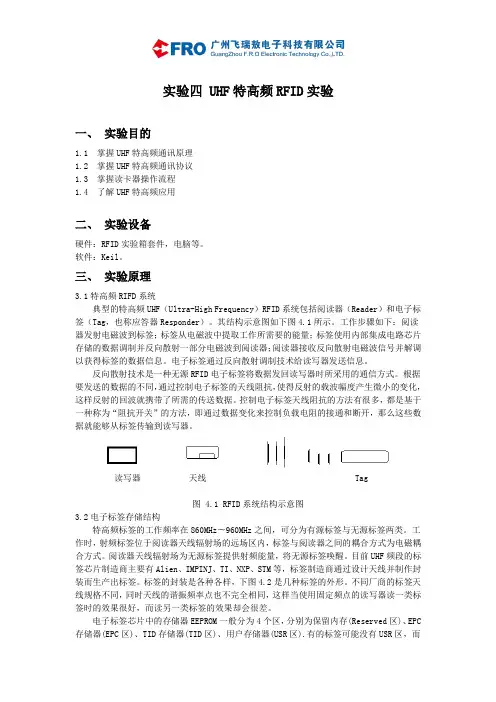
其结构示意图如下图4.1所示。
工作步骤如下:阅读器发射电磁波到标签;标签从电磁波中提取工作所需要的能量;标签使用内部集成电路芯片存储的数据调制并反向散射一部分电磁波到阅读器;阅读器接收反向散射电磁波信号并解调以获得标签的数据信息。
电子标签通过反向散射调制技术给读写器发送信息。
反向散射技术是一种无源RFID电子标签将数据发回读写器时所采用的通信方式。
根据要发送的数据的不同,通过控制电子标签的天线阻抗,使得反射的载波幅度产生微小的变化,这样反射的回波就携带了所需的传送数据。
控制电子标签天线阻抗的方法有很多,都是基于一种称为“阻抗开关”的方法,即通过数据变化来控制负载电阻的接通和断开,那么这些数据就能够从标签传输到读写器。
读写器天线 Tag图 4.1 RFID系统结构示意图3.2电子标签存储结构特高频标签的工作频率在860MHz〜960MHz之间,可分为有源标签与无源标签两类。
工作时,射频标签位于阅读器天线辐射场的远场区内,标签与阅读器之间的耦合方式为电磁耦合方式。
阅读器天线辐射场为无源标签提供射频能量,将无源标签唤醒。
目前UHF频段的标签芯片制造商主要有Alien、IMPINJ、TI、NXP、STM等,标签制造商通过设计天线并制作封装而生产出标签。
标签的封装是各种各样,下图4.2是几种标签的外形。
不同厂商的标签天线规格不同,同时天线的谐振频率点也不完全相同,这样当使用固定频点的读写器读一类标签时的效果很好,而读另一类标签的效果却会很差。
UHF RFID芯片 AS3990-AS3991芯片资料

AS3990/AS3991UHF RFID Single Chip Reader EPC Class1 Gen2 CompatibleD a ta S h e e t1 General DescriptionThe AS3990/AS3991 UHF reader chip is an integrated analog front end and protocol handling systems for a ISO18000-6C 900MHz RFID reader system.Equipped with built-in programming options, the device is suitable for a wide range of UHF RFID applications. The R901G includes improved on-board VCO and internal PA.The reader configuration is achieved by selecting the desired protocol in control registers. Direct access to all control registers allows fine tuning of different reader parameters.Parallel or serial interface can be selected forcommunication between the host system (MCU) and the reader IC. When hardware coders and decoders are used for transmission and reception, data is transferred via 24 bytes FIFO register.In case of direct transmission or reception, coders and decoders are bypassed and the host system can service the analog front end in real time.The transmitter generates 20dBm output power into 50Ω load and is capable of ASK or PR-ASK modulation. The integrated supply voltage regulators ensure supply rejection of the complete reader system.The transmission system comprises low level datacoding. Automatic generation of FrameSync, Preamble, and CRC is supported.The receiver system allows AM and PM demodulation. The receiver also comprises automatic gain control option (patent pending) and selectable gain and signal bandwidth to cover a range of input link frequency and bit rate options.The signal strength of AM and PM modulation is measured and can be accessed in RSSI register.The receiver output is selectable between digitized sub-carrier signal and any of integrated sub-carrierdecoders. Selected decoders deliver bit stream and data clock as outputs.The receiver system also comprises framing system. This system performs the CRC check and organizes the data in bytes. Framed data is accessible to the host system through a 24 byte FIFO register.To support external MCU and other circuitry a 3.3V regulated supply and clock outputs are available. The regulated supply has 20mA current capability.The AS3990/AS3991 is available in a 64-pin QFN (9mm x 9mm), ensuring the smallest possible footprint.2 Key FeaturesISO18000-6C (EPC Gen2) full protocol support ISO18000-6A,B compatibility in direct mode Integrated low level transmission coding Integrated low level decoders Integrated data framing Integrated CRC checkingParallel 8-bit or serial 4-pin SPI interface to MCUusing 24 bytes FIFOVoltage range for communication to MCU between1.8V and 5.5VSelectable clock output for MCUIntegrated supply voltage regulator (20mA), whichcan be used to supply MCU and other external circuitryIntegrated supply voltage regulator for the RF outputstage, providing rejection to supply noiseInternal power amplifier (20dBm) for short rangeapplicationsModulator using ASK or PR-ASK modulation Adjustable ASK modulation index AM & PM demodulation ensuring no“communication holes” with automatic I/Q selectionBuilt-in reception low-pass and high-pass filters having selectable corner frequenciesSelectable reception gain Reception automatic gain controlAD converter for measuring TX power usingexternal RF power detectorDA converter for controlling external power amplifier Frequency hopping supportOn-board VCO and PLL covering complete RFIDfrequency range 840MHz to 960MHzOscillator using 20MHz crystal Power down, standby and active mode Can be powered by USB with no need for stepconversion3 ApplicationsThe device is an ideal solution for UHF RFID readersystems and hand-held UHF RFID readers.Figure 1. Block DiagramContents1 General Description (1)2 Key Features (1)3 Applications (1)4 Pin Assignments (5)Pin Descriptions (5)5 Absolute Maximum Ratings (8)6 Electrical Characteristics (9)7 Detailed Description (11)Supply (11)Power Modes (12)Host Communication (13)VCO and PLL (13)VCO and External RF Source (13)PLL (13)Chip Status Control (14)Protocol Control (14)Option Registers Preset (14)Transmitter (14)Normal Mode (14)Direct Mode (16)Modulator (17)Amplifier (17)Receiver (18)Input Mixer (18)RX Filter (18)RX Gain (19)Received Signal Strength Indicator (RSSI) (19)Reflected RF Level Indicator (19)Normal Mode (19)Direct Mode (21)Normal Mode With Mixer DC Level Output And Enable RX Output Available (21)ADC / DAC (21)DA Converter (21)AD Converter (22)Reference Oscillator (22)8 Application Information (23)Configuration Registers Address Space (23)Main Configuration Registers (24)Control Registers - Low Level Configuration Registers (25)Status Registers (30)Test Registers (32)PLL, Modulator, DAC, and ADC Registers (33)RX Length Registers (37)FIFO Control Registers (38)Direct Commands (39)Idle (80) (40)Soft Init (83) (40)Hop to Main Frequency (84) (40)Hop to Auxiliary Frequency (85) (40)Trigger AD Conversion (87) (40)Reset FIFO (8F) (40)Transmission With CRC (90) (40)Transmission With CRC Expecting Header Bit (91) (40)Transmission Without CRC (92) (41)Delayed Transmission With CRC (93) (41)Delayed Transmission Without CRC (94) (41)Block RX (96) (41)Enable RX (97) (41)EPC GEN2 Specific Commands (41)Query (98) (41)QueryRep (99) (41)QueryAdjustUp (9A) (41)QueryAdjustNic (9B) (41)QueryAdjustDown (9C) (42)ACK (9D) (42)NAK (9E) (42)ReqRN (9F) (42)Reader Communication Interface (42)Parallel Interface Communication (44)Serial Interface Communication (46)Timing Diagrams (47)Timing Parameters (48)FIFO (48)9 Package Drawings and Markings (49)10 Ordering Information (50)4 Pin AssignmentsPin DescriptionsTable 1. Pin DescriptionsPin Name Pin Number Pin Type Description COMN_A1BIDConnect de-coupling capacitor to VDD_5LFI COMP_B2BIDCOMN_B3BIDDAC4OUT DAC output for external amplifier support, Output Resistance of DAC pin is 1kΩVDD_5LFI5SUPI Positive supply for LF input stage, connect to VDD_MIX VSS6SUPI SubstrateMIX_INP7INP Differential mixer positive inputVSS8SUPI SubstrateMIX_INN9INP Differential mixer negative inputMIXS_IN10INP Single ended mixer inputVSN_MIX11SUPI Mixer negative supplyCBIB12BID Internal node de-coupling capacitor to GNDVDD_MIX13SUPO Mixer positive supply, internally regulated to 4.8VCBV514BID Internal node de-coupling capacitor to VDD_MIXVDD_TXPAB15SUPI Power Amplifier Bias positive supply. Connect to VDD_MIX VEXT 16SUPI Main positive supply input (5…5.5V)VEXT217SUPI PA positive supply regulator input (2.5… 5.5V)VDD_RF 18SUPO PA positive supply regulator output, internally regulated to 2…3.5V VDD_B 19SUPO PA buffer positive supply. Internally regulated to 3.4V RFOUTP_1201OUT PA positive RF outputRFOUT1 and RFOUT2 must be tied togetherRFOUTP_2211OUT VSN_1221SUPI PA negative supplyVSN_2231SUPI VSN_3241SUPI VSN_4251SUPI VSN_5261SUPI RFOUTN_1271OUT PA negative RF output or used in single ended mode.RFOUT1 and RFOUT2 must be tied together RFOUTN_2281OUT VSN_D 29SUPO Digital negative supplyOAD230BID Analog or digital received signal output and MCU support mode sense inputOAD 31BID Analog or digital received signal output RFONX 32OUT Low power linear negative RF output (~0dBm)RFOPX 33OUT Low power linear positive RF output (~0dBm)VDD_RFP 34SUPO RF path positive supply, internally regulated to 3.4V VSN_RFP 35SUPI RF path negative supply OSCI 36INP Crystal oscillator inputOSCO 37BID Crystal oscillator output or external 20MHz clock input VDD_D 38SUPO Digital part positive supply, internally regulated to 3.4V EN 39INP Enable input IRQ 40OUT Interrupt outputIO041BID I/O pin for parallel communication IO142BID IO243BID I/O pin for parallel communicationEnableRX input in case of direct mode IO344BID I/O pin for parallel communicationModulation input in case of direct modeIO445BID I/O pin for parallel communicationSlave select in case of serial communication (SPI)IO546BIDI/O pin for parallel communicationSub-carrier output in case of direct modeTable 1. Pin Descriptions Pin Name Pin NumberPin Type DescriptionNotes:1. BID: Bidirectional pin2. INP: Input pin3. OUT: Output pin4. SUPI: Supply Input pin5. SUPO: Supply Output pin .IO647BIDI/O pin for parallel communication.MISO in case of serial communication (SPI)Sub-carrier output in case of direct mode IO748BID I/O pin for parallel communication.MOSI in case of serial communication (SPI)CLSYS 49OUT Clock output for MCU operationCLK 50INP Clock input for MCU communication (parallel and serial)VDD_IO 51SUPI Positive supply for peripheral communication, connect to host positive supplyCD252BID Internal node de-coupling capacitor CD153BID AGD 54BID Analog reference voltage VSN_A 55SUPI Analog part negative supplyEXT_IN 56INP RF input in case external VCO is used VSN_CP 57SUPI Charge pump negative supplyADC 58IN ADC input for external power detector support VDD_A 59SUPO Analog part positive supply, internally regulated to 3.4V VCO 60INP VCO inputVOSC 61BID Internal node de-coupling capacitor CP 62OUT Charge pump outputVDDLF 63SUPI Positive supply for LF processing, internally regulated to 3.4COMP_A 64BID Internal node, connect de-coupling capacitor to VDD_5LFI EXP_PAD65SUPIExposed paddle, must be tied to GND1.Internal Power amplifier is not available on AS3990.Table 1. Pin Descriptions Pin Name Pin NumberPin Type DescriptionData Sheet - A b s o l u te M a x i m u m R a ti n g s5 Absolute Maximum RatingsStresses beyond those listed in Table 2 may cause permanent damage to the device. These are stress ratings only, and functional operation of the device at these or any other conditions beyond those indicated in ElectricalCharacteristics on page 9 is not implied. Exposure to absolute maximum rating conditions for extended periods may affect device reliability.Table 2. Absolute Maximum RatingsParameter MinMax Units CommentsSupply voltage, V EXT 5.5V Positive voltage other pads V S ± 0.3V Negative voltage other pads-0.3V Output current, I O±100mA Maximum junction temperature T J 125ºC The maximum junction temperature for continuous operation is limited by packageconstraints.Storage temperature range, T stg-55+150ºCLead temperature 1,6 mm (1/16 inch)from case for 10 seconds260ºCThe reflow peak soldering temperature(body temperature) is specified according IPC/JEDEC J-STD-020C“Moisture/Reflow Sensitivity Classification for non-hermetic Solid State Surface Mount Devices”.ESD rating11.This integrated circuit can be damaged by ESD. We recommend that all integrated circuits are handled with appropriate precautions. Failure to observe proper handling and installation procedures can cause damage. ESD damage can range from subtle performance degradation to complete device failure. Precision integrated circuits may be more susceptible to damage because very small parametric changes could cause the device not to meet the published specifications. RF integrated circuits are also more susceptible to damage due to use of smaller protection devices on the RF pins, which are needed for low capacitive load on these pins.IO pins, HBM 2kV RF pins, HBM1kV6 Electrical CharacteristicsV EXT = 5.3V, typical values at 25ºC, unless otherwise noted.Table 3. Electrical CharacteristicsSymbol Parameter Conditions Min Typ Max UnitsI VEXT Supply current without PAdriver currentV EXT Consumption80mAI VEXT+I VEXT2Supply Current for AS3991 andinternal PA11.Internal PA is available on AS3991only.V EXT2 Consumption,V EXT2 = 2.5V310mAI STBY Standby current3mAI PD Supply current in power-downmode All system disabled includingsupply voltage regulators20100µA210V AGD AGD voltage 1.5 1.6 1.7V V POR Power on reset voltage (POR) 1.4 2.0 2.5VV VDD Regulated supply for internalcircuitry and for external MCU 3.2 3.4 3.6VV DD RF Regulated supply for internalPA 1.92 2.1VV VDD MIX1Regulated supply for mixers, bitvext_low=LThe difference between theexternal supply and the regulatedvoltage is higher than 250mV4.5 4.85.1VV VDD MIX2Regulated supply for mixers, bitvext_low=HThe difference between theexternal supply and the regulatedvoltage is higher than 250mV3.5 3.7 3.9VP PSSR Rejection of external supplynoise on the supply regulatorsThe difference between theexternal supply and the regulatedvoltage is higher than 250mV26dBP RFAUX Auxiliary output power0dBm P RFOUT Internal PA output power120dBm R RFIN RFIN input resistance100ΩV SENS Input sensitivity-66dBm 1dB CP Input 1dB compression point10dBm IP3Third order intercept point21dBm T REC Recovery time after modulation Maximum LF selected10µs Logic Input/OutputMax. CLK frequency1MHz V LOW Input logic low0.2V DD_IO V HIGH Input logic high0.8V DD_IO R IO Output resistance IO0…IO7low_io = H for VDD_IO<2.7V400800ΩR CL SYS Output resistance CL SYS low_io = H for VDD_IO<2.7V200ΩTable 4. Recommended Operating ConditionsSymbol Parameter Conditions Min Typ Max Units Supply Voltage 5.0 5.3 5.5V Supply voltage (bit vext_lowset) 4.1VT J Operating virtual junctiontemperature range-40125ºC T AMB Ambient temperature-4085ºC Rth junction to exposed die padº/W7 Detailed DescriptionThe RFID reader IC comprises complete analog and digital functionality for reader operation including transmitter and receiver section with complete EPC Gen2 or ISO18000-6C digital protocol support. To integrate as many components as possible, the device also comprises an on-board PLL section with integrated VCO, supply section, DAC and ADC section, and host interface section. In order to cover a wide range of possibilities, there is also Configuration registers section that configures operation of all blocks.For operation, the device needs to be correctly supplied via. VEXT and VEXT2 pins and enabled via. EN pin (Refer Supply on page 11 for connecting to supply and Power Modes on page 12 about operation of the EN pin). At power-up the configuration registers are preset to a default operation mode. The preset values are described in the Configuration Registers Address Space on page 23 below each register description table. It is possible to access and change registers to choose other options.The communication between the reader and the transponder follows the reader talk first method. After power-up and configuring IC, the host system starts communication by turning on the RF field by setting option bit rf_on in the ‘Chip status control register’ (00) (see Table 13) and transmitting the first protocol command (Select in EPC Gen2). Transmitting and receiving is possible in the following two modes:1. Normal Data Mode: In this mode, the TX and RX data is transferred through the FIFO register and all protocoldata processing is done internally.2. Direct Data Mode: In this mode, the data processing is done by the host system.SupplyThe effective supply system of the chip decreases the influence of the supply noise and interference and thus improves de-coupling between different building blocks. A set of 3.4V regulators is used for supplying the reference block, AD and DA converters, low frequency receiver cells, the RF part, and digital part. It is possible to use the digital part supply VDD_D for supplying the external MCU with a current consumption up to 20mA. The input pin for the regulators is VEXT. The output pins for regulators are VDD_A, VDD_LF, VDD_D, VDD_RFP and VDD_B. Each of the pins require stabilizing capacitors to connected ground (2.2…10µF and 10…100nF) in parallel. Depending on quality of the capacitors, 100pF could be required.An additional 4.8V regulator is used for the input RF mixers supply. The input of this regulator is VEXT, output is VDD_MIX pin. For correct operation of the 4.8V regulator, the VEXT voltage needs to be between 5.3V and 5.5V. VDD_MIX needs de-coupling capacitors to VDD_MIX like other VDD pins.In case lower VEXT supply voltage is used (down to 4.1V), two option bits have to be set to optimize the chip performance to the lower supply. The vext_low in the ‘TRcal high and misc register’ (05) bit decreases VDD_MIX voltage to 3.7V to maintain the regulators PSSR and the ir<1> bit in the ‘RX special setting 2’ (0A) adapts mixer’s internal operating point to lower supply. Adaptation to low supply is implemented in differential mixer only. The consequence of the decreased supply is lower mixer’s input range.VDD_5LFI and VDD_TXPAB pins are supply input pins and should be connected to VDD_MIX. The internal 20dBm power amplifier 1has an internal regulator from 2…3.5V. The output voltage selection is done by reg2v1:0 option bits in the ‘Regulator and IO control register’ (0B) (see Table 24).The input pin is VEXT2 and output is VDD_RF. For optimum noise rejection performance, the input voltage at VEXT2 pin needs to be at least 0.5V above the regulated supply output. Connecting VEXT2 directly to VEXT is possible only at the expense of increasing IC’s power dissipation and decreasing the maximum operating temperature.A separate I/O supply pin (VDD_IO) is used to supply the internal level shifters for communication interface to the host system (MCU). VDD_IO should be connected to MCU supply to ensure proper communication between the chip and MCU. In case the MCU is supplied by VDD_D from the reader IC also VDD_IO should be connected to VDD_D.Power ModesThe chip has three power modes.Power Down Mode: The power down mode is activated by EN pin low (EN=L). For correct operation, the OAD2pin should not be connected.Normal Mode: The normal mode is entered by EN=H. In this case all supply regulators, reference voltage system,crystal oscillator, RF oscillator and PLL are enabled. After the crystal oscillator stabilizes, the CLSYS clock becomes active (default frequency is 5MHz) and the chip is ready to move to transmit or receive operation.Standby Mode: The standby mode is entered from normal mode by option bit stby=H. In the standby mode theregulators, reference voltage system, and crystal oscillator are operating in low power mode; but the PLL,transmitter output stages and receiver are switched off. All the register settings are kept while switching between standby and normal mode.Power Down with MCU Support mode intends to support the MCU if the majority of the reader IC is in power down. This mode is enabled by connecting 10k Ω resistor between OAD2 pin and ground. During EN=L period, the VDD_D regulator is enabled in low power mode and the CLSYS frequency is 60kHz typically.It is also possible to trigger temporary normal mode from power down mode (EN=L) by pulling shortly the OAD2 pin low via 10k Ω or less. After the crystal oscillator is stable and the CLSYS clock output is active, the chip waits for approximately 200µs and then changes back to the power down mode. Using this function, the superior system can wake up the reader IC and MCU that are both in the power down mode. If the MCU during 200µs period finds out that the RFID system must react, it confirms the normal mode by setting EN high.1.Internal PA is available on AS3991only.Table 5. AS3990/AS3991 Power ModesPower mode EN OAD2Std by Power down L -X Power down SYSCLK of 60kHz L 10k to GNDX Normal power HX X Stand by XH Listen modeL 10k and falling edgeXHost CommunicationAn 8-bit parallel interface (pins IO0 to IO7) with two control signals (CLK, IRQ) forms the main communication system. It can also be changed (by hardwiring some of the 8 I/O pins) to a serial interface. The data handling is done by a 24 byte FIFO register used in both directions, transmission and reception. For more details, refer Reader Communication Interface on page 42.The signal level for communication between the host system (MCU) is defined by the supply voltage connected to VDD_IO pin. Communication is possible in wide range between 1.8V and 5.5V. In case the pull-up output resistance at VDD_IO below 2.7V is to high, it can be decreased by setting option bit vdd_io_low in the ‘TRcal High and Misc register’ (05). In case the MCU is supplied from the reader IC, then both the MCU supply and VDD_IO pin need to be connected to VDD_D.CLSYS output level is defined by the VDD_IO voltage. It is also possible to configure CLSYS to open drain N-MOS output by setting the option bit open_dr in the in the ‘TRcal high and misc register’ (05), (see Table 18). This function can be used to decrease amplitude and harmonic content of the CLSYS signal and decrease the cross-talk effects that could corrupt operation of other parts of the circuit.VCO and PLLThe PLL section is composed of a voltage control oscillator (VCO), prescaler, main and reference divider, phase-frequency detector, charge pump, and loop filter. All building blocks excluding the loop filter are completely integrated. Operating range is 860MHz to 960MHz.VCO and External RF SourceInstead of the internal PLL signal, an external RF source can be used. The external source needs to be connected to EXT_IN pin and option bit eext_in in the ‘PLL A/B divider auxiliary register‘ (17) (see Table 36) needs to be set high. The EXT_IN input optimum level is 0dBm with a DC level between 0V and 2V.It is also possible to use external VCO and internal PLL circuitry. In this case, the output of the external VCO (0dBm) needs to be connected to EXT_IN, option bits eext_in and epresc in the ‘PLL A/B divider auxiliary register’ (17) both need to be set high. The charge pump output pin CP needs to be connected to the external loop filter input and loop filter output to the external VCO input. This configuration is useful in case the application demands better phase noise performance than the completely integrated oscillator offers.The internal on-board VCO is completely integrated including the variable capacitor and inductor. The control input is pin VCO; input range is between 0 and 3.3V. The option bits eosc<2:0> in the ‘CLSYS, analog out and CP control’ (14) (Table 33) can be used for oscillator noise and current consumption optimization. Option bit lev_vco in the ‘PLL A/B divider auxiliary register’ (17) (see Table 36) is used to optimize the internal VCO output level to other RF circuitry demands. VCO and CP pin valid range is between 0.5V and 2.9V.AS3991 and above have internal VCO set to a frequency range around 1800MHz, later internally divided by two for decreasing the VCO pulling effect. The tuning curve of 1800MHz VCO is divided into 16 segments to decrease VCO gain and attain lowest possible phase noise.Configuration of the 1800MHz VCO tuning range can be manual using option bits vco_r<3:0> in the ‘CL_SYS, analog out and CP control’ register (14) or automatic using L-H transition on option bit auto in the same register. The device allows measurement of the VCO voltage using option bit mvco and reading out the 4 bits result of the automatic segment selection procedure, both in the same register.PLLThe divide by 32/33 prescaler is controlled by the main divider. The main divider ratio is defined by the ‘PLL A/B divider main register’ (16). The low ten bits in the three bytes deep register define A value and the next ten bits define B value. The A and B values define the main divider division ratio to N=B*32+A*33. The reference clock is selectable by RefFreq<2:0> bits in the ‘PLL R, A/B divider main register’ (16) (see Table 35). The available values are 500 kHz, 250 kHz, 200 kHz, 100 kHz, 50 kHz, 25 kHz. Charge pump current is selectable between 150µA and 1200µA using option bits cp1:0 in the ‘CL_SYS, analog out and CP control register’ (14) (see Table 33). The cp<3> is used to change the polarity (direction) of the charge pump output.The frequency hopping is supported by direct commands ‘Hop to main frequency’ (84) and ‘Hop to auxiliary frequency’ (85). The hopping is controlled by host system (MCU) using two configuration registers for two frequencies. Before enabling the RF field, the host system needs to configure the PLL by writing the ‘CL_SYS, analog out and PLL register’ (09) and the ‘PLL R, A/B divider main’ (16) registers. Any time during operating at the first selected frequency, the external system can configure the three bytes deep ‘PLL A/B divider auxiliary (17)’ register.Hopping to the second frequency is triggered, if direct command ‘Hop to auxiliary frequency’ is sent. Hop to the third frequency is similar: the register ‘PLL A/B divider main (16)’ can be written any time the external system has free resources and actual hop is triggered by direct command ‘Hop to main frequency’.Chip Status ControlIn the ‘Chip status control register’ (00) (see Table 13), main functionality of the chip is defined. By setting the rf_on bit in the ’Chip control register’ (00), the transmit and receive part are enabled. The initial RF field ramp-up is defined with the Tari1:0 option bits in the ‘Protocol control register’ (01) (see Table 14). It is also possible to slow down the initial RF field ramp by option bits trfon1:0 in the ‘Modulator control register’ (15) (see Table 34). The available values are 100µs, 200µs, and 400µs.The host system can check whether the field ramp-up is finished via the rf_ok bit in the ‘AGC and internal status register’ (0E) (see Table 27), which is set high when ramp-up is finished. By setting the rf_on bit low, the field will ramp-down similarly to the ramp-up transient. It is also possible to enable receiver operation by setting rec_on bit. Theagc_on and agl_on bits enables the (Automatic Gain Control) AGC and (Automatic Gain Leveling) AGL functionality, dac_on enables DA converter, bit direct enables the direct data mode, and stby bit moves chip to the stand-by power mode.Protocol ControlIn the ‘Protocol control register’ (01) (see Table 14), the main protocol parameters are selected (Tari value and RX coding for EPC Gen2 protocol). The Gen2 Protocol is configured by setting Prot<1:0> bits to low. The dir_mode<6> bit defines type of output signals in case the direct mode is used. The rx_crc_n<7> bit high defines reception in case the user does not want to check CRC internally. In this case, the CRC is not checked but is just passed to the FIFO like other data bytes. In the EPC Gen2, this function is useful in case of truncated EPC reply where the ‘CRC’ transponder transmits is not valid CRC calculated over actual transmitted data.Option Registers PresetAfter power up (EN low to high transition), the option registers are preset to values that allow default reader operation. Default transmission uses Tari 25µs, PW length is 0.5Tari, TX one length is 2 Tari, and RTcal is 133µs. Default reception uses FM0 coding with long preamble, link frequency 160kHz. Default operation is set to internal PLL with internal VCO, differential input mixers, low power output (RFOPX, RFONX), and DSB-ASK transmit modulation. TransmitterTransmitter section comprises of protocol processing digital part, shaping, modulator and amplifier circuitry. The RF carrier is modulated with the transmit data and amplified for transmission.Normal ModeIn normal mode, all signal processing (protocol coding, adding preamble or frame-sync and CRC, signal shaping, and modulation) is done internally.The external system (MCU) triggers the transmission and loads the transmit data into the FIFO register. The transmission is started by sending the transmit command followed by information on the number of bytes that should be transmitted and the data. The number of bytes needs to be written in the ‘TX length’ registers and the data to the FIFO register. Both can be done by a single continuous write. The transmission actually starts when the first data byte is written into the FIFO.The second possibility is to start transmission with one of the direct Gen2 commands (Query, QueryRep, QueryAdjust, ACK, NAK, ReqRN). In this case, the transmission is started after receiving the command.In case the transmission data length is longer than the size of the FIFO, the host system (MCU) should initially fill the FIFO register with up to 24 bytes. The reader chip starts transmission and sends an interrupt request when only 3 bytes are left in the FIFO. When interrupt is received, the host system needs to read the ‘IRQ status register’ (0C) (see Table 25). By reading this register, the host system is notified by the cause of the interrupt and the same reading also clears the interrupt. In case the cause of the interrupt is low FIFO level and the host system did not put all data to the FIFO, the remaining data needs to be sent to FIFO, again according to the available FIFO size. In case all transmission data was already sent to the FIFO, the host system waits until the transmission runs out. At the end of the transmit operation, the external system is notified by another interrupt request with a flag in the IRQ register that signals the end of transmission.。
Impinj 英频杰产品手册
•
遵循 EPCglobal UHF Class 1 Gen 2 / ISO 18000-6C
协议
•
输出功率:+10.0 到 +30.0 dBm (POE 供电),+10.0
到 +32.5 dBm(外部电源供电),功率可调
•
-82dBm 业界最高接收灵敏度,接收灵敏度可调
•
2 个收发一体 RP TNC 天线接口
RFID 工作频段
•
内置功放+20dBm 最大输出,可配合使用外置功放,
5
Indy R2000 Chips Indy R500 Chips
Part Number
可配置数字基带
•
发射相位噪声-116 dBm/Hz@250kHz
•
-75 dBm 接收灵敏度(+5dBm 载波泄漏,DRM 模
式)
•
相关接收机架构保证了稳定的 RSSI 值以及可信的载波
Part Number IPJ-A0402-USA
Part Number IPJ-A0303-000
描述
Guardwall(FCC)(70×40×10 cm)
•
工作频段:902-928 MHz
•
极化方式:左旋和右旋极化(内置两种极化单元),
3dB 轴比(最大)
•
远场增益:+6 dBi
•
半功率波瓣宽度:55 度
可配置数字基带
•
发射相位噪声-126 dBm/Hz@250kHz
6
Indy R2000 Dev Platform
Indy R1000 Dev Platform Indy Source Code License
Impinj 产品技术交流(20111028)(1)

E41C
95×8
E44 E42
105×6
68×19
H47 (True 3D)
44×44
服装,零售业,资产管理,物流
可达10m以 上
24
Monza 5 Inlay
• Monza 5系列Inlay
主要应用于服装行业,同时也应用于资产管理物流等环节
Inlay图片
型号
尺寸(mm) 应用读取距离Fra bibliotekE51
95×8
• 最大第二代UHF技术合作伙伴社区
– Impinj公司通过合作伙伴销售其产品
18
标签芯片&Inlay
19
Impinj Monza标签芯片
• ~75%标签芯片市场份额
– 销售量已达36亿片 – 晶圆或已封装芯片
• 最佳质量,最佳性能,最可靠
– 99.97%转换后成品率 – 双天线xyz 3-轴读写 – 写入速度可达2000标签/分钟
12
RFID发展历程
• • • • • • 1941~1950 年:雷达的改进和应用催生了RFID 技术,1948 年奠定了RFID 技术的理论基础。 1951—1960 年:早期RFID 技术的探索阶段,主要处于实验室实验研究。 1961—1970 年:RFID 技术的理论得到了发展,开始了一些应用尝试。 1971—1980 年:RFID 技术与产品研发处于一个大发展时期,各种RFID 技 术测试得到加速。出现了一些最早的RFID 应用。 1981~1990 年:RFID 技术及产品进入商业应用阶段,各种规模应用开始出 现。 1991~2000 年:RFID 技术标准化问题日趋得到重视,RFID 产品得到广泛 采用,RFID 产品逐渐成为人们生活中的一部分。 2001—今:标准化问题日趋为人们所重视,RFID 产品种类更加丰富,有源 电子标签无源电子标签及半无源电子标签均得到发展,电子标签成本不断降 低,规模应用行业扩大。
倍福RFID读写器手册说明书

Company AddressesEurope, Germany, HeadquarterBalluff GmbHSchurwaldstraße 9D-73765 Neuhausen a.d.F.ArgentinaBalluff Argentina S.R.L.Av del Libertador 650 Piso 7 SurB1638BES - Vicente Lopez, Buenos AiresAustraliaBalluff Pty Ltd.18 Malvern StreetBayswater, 3153 VictoriaBrasilBalluff Controles Elétricos Ltda.Rua Francisco Foga, 25 ,Distrito IndustrialCEP 13280.000 – Vinhedo – SPCanadaBalluff Canada Inc.2840 Argentia Road, Unit 1 Mississauga,Ontario L5N 8G4ChinaBalluff (Shanghai) Trading Co. Ltd.No.800 Chengshan Rd, 8F, Building A, Yunding International Commercial Plaza 200125, Pudong, ShanghaiJapanBalluff Co., Ltd.Aqua Hakusan Bldg. 9F 1-13-7 Hakusan, Bunkyo-ku,Tokyo 113-0001MexicoBalluff de México S.A. de C.V.Anillo Vial II Fray Junipero Serra No. 4416; Colonia La Vista ResidencialCP 76232 Delegación Epigmenio González, QuerétaroUSABalluff Inc.8125 Holton Drive, FlorenceKentucky 41042-0937Operating GuidePurpose of the DeviceThe BF-IDU08 device is intended to read and write "EPC Global Class 1 Gen2" compliant data carriers (so called tags) via country dependent UHF radio frequencies.Check that you have the right device variantThis UHF system consists of a radio frequency unit and an integrated antenna according to specifications and may only be operated within the specified countries subject to all applicable national legal regulations and standards.Check that the type label contains the correct type of approval symbol for your country.► When using the UHF system in the European Community, the provisions in ETSI standard 302 208 apply.► When using the UHF system in the USA, the directives of the FCC, Part 15 B and 15 C, apply.► When using the UHF system in Canada, the directives of the IC, RSS-210 apply.► When using the UHF system in China, the directives of the RFID National Standard and GB 9254 apply.This device complies with Part 15 of the FCC Rules. Operation is subject to the following two conditions:(1) This device may not cause harmful interference, and(2) This device must accept any interference received, including interference that may cause undesired operation.Connecting the DeviceThe BF-IDU08 device has to be connected to one of the IO-Link-Device ports of an IO-Link-Master unit via standard 4-wire cable with M12 industry connectors (A-coded). The IO-Link-Master unit provides power supply and controls the device over its IO-Link interface connection.Figure 1: System overviewThe IO-Link-Master unit itself needs to be connected to a power supply and the customer's PLC unit. For further information, please refer to the user manual of the used IO-Link-Master unit. MountingBefore operating the device has to be mounted with the provided M30 nuts or other suitable fixtures, Figure 2. Optional mounting fixtures are available at .The BF-IDU08 device may be mounted in any direction, the operating direction of the integrated antenna is towards the length axis of the BF-IDU08 device as displayed in Figure 1 (direction towards the UHF-Tags).Figure 2: BF-IDU08 mounted on metal carrier using 2 x Nut M30The antennas of the identification system BIS U transmit ultra-high frequency electromagnetic waves. People should not remain within the near enclosure of the UHF antenna over long time periods (several hours). The mounting position of the BF-IDU08 should take respect to a clearance area of about 25cm to workplaces.Setup and OperationThe BF-IDU08 device will operate when connected to an IO-Link-Master that provides power supply and implements the BF-IDU08 RFID-Reader protocol.Device behavior e.g. transmission power or operating modes can be setup via different parameters. Protocol description and available parameters are described in the firmware configuration manual.Status IndicatorsThe device will show its status using RGB LEDs located at the M12 plug. Depending on the device state the LED changes color and lighting mode (static, blink slow, blink fast).Electrical DataMechanical Data。
D100使用说明书

目录一、认识您的读写器 (3)1.1前视图 (3)1.2后视图 (3)1.3俯视图 (3)二、读写器的操作和设置 (4)2.1初次使用 (4)2.1.1 第一步:连接数据线 (4)2.1.2 第二步:用演示软件操作读写器 (5)2.2射频参数设置 (7)2.2.1设置射频输出功率 (7)2.3 盘存ISO-18000-6C标签 (7)2.3.1缓存模式和实时模式 (7)2.4存取 ISO-18000-6C标签 (12)2.4.1读标签操作 (12)2.4.2写标签操作 (13)2.4.3锁定标签操作 (14)2.4.4灭活标签操作 (14)2.4.5选定操作的标签 (15)三、开发自己的RFID应用程序 (16)四、安装驱动 (17)一、认识您的读写器1.1前视图1.2后视图1.3俯视图二、读写器的操作和设置2.1初次使用2.1.1 第一步:连接数据线通过USB数据线与电脑连接,如图:此时,需要将配置开关切换到如下图所示位置:也可以通过串口与电脑相连,如图:此时,需要将配置开关切换到如下图所示位置:连接好读写器的同时,将听到“滴”的一声鸣响,同时指示灯亮。
表示上电过程正常,读写器自检通过。
注:读写器首次与PC连接会自动安装驱动。
如过驱动安装失败,可以到我司网站下载驱动并手动安装。
(安装方法详见:第15页“安装驱动”)2.1.2 第二步:用演示软件操作读写器启动随机附带的演示软件。
此软件不需要安装,直接将 UHFDemo.exe , reader.dll, customControl.dll 三个文件拷贝至同一个文件夹,并双击可执行文件 UHFDemo.exe 即可。
软件启动后界面如图所示:选择对应的串口号(查看串口号:我的电脑-管理-设备管理器-端口-USB Serial Port),然后单击“连接读写器”按钮,若串口没有被占用,在下方的操作记录栏里会显示如下信息:单击读取版本号按钮,界面将显示相应的信息,如下图所示:此时,读写器与电脑的连接已成功完成。
UHF频段RFID天线的小型化设计与分析
UHF频段RFID天线的小型化设计与分析一、综述随着无线通信技术的飞速发展,RFID(无线射频识别)技术已广泛应用于各个行业,从物流追踪、库存管理到门禁系统等。
特别是在UHF(超高频)频段,RFID系统的读写距离和读取速度得到了显著的提升,使其成为物联网领域备受关注的通信技术之一。
RFID系统主要由RFID阅读器(读写器)和RFID标签(电子标签)组成。
在UHF 频段,RFID阅读器和标签之间的能量传输主要依赖于天线。
传统RFID 天线由于尺寸大、损耗大等问题,在实际应用中逐渐暴露出性能不足的问题。
对UHF频段RFID天线进行小型化设计与分析显得至关重要。
天线的工作原理与性能参数:首先介绍RFID天线的基本工作原理,以及影响其性能的主要参数,如增益、驻波比、效率等。
小型化设计方案:探讨在UHF频段实现RFID天线小型化的各种途径,包括采用截断正方形贴片天线的SRR负载的超材料、开槽环谐振天线、截断正六边形贴片天线等。
同时将几种方案应用于实际中评估性能。
性能分析: 讨论在上述小型化方案中,如何优化设计以提高天线的性能,如提高方向性、减少互扰、降低损耗等,并分析这些方法在实际应用中的优势和局限性。
仿真实验与实际测试:通过使用电磁场仿真软件对小型化RFID天线进行初步设计估计,然后通过实际制作和测试对比实验数据,来验证改进方案的有效性和可行性。
_______技术简介RFID(Radio Frequency Identification,射频识别)技术是一种基于无线射频通信的非接触式识别技术。
它通过无线电讯号识别特定目标并读写相关数据,而无需建立机械或光学接触。
RFID系统通常由标签(Tag)、读取器(Reader)和后端管理系统组成。
在RFID应用中,当标签进入阅读器的射频场范围内时,标签会自动激活并与读取器进行通信。
标签内包含了可编程的存储器和天线,用于存储信息、识别码以及接受命令。
读取器发送的无线电波能量会激发标签内的电路,使其能够传输存储在其中的唯一识别信息。
RFID读写器
6.3 读写器的结构形式
2.发卡机
发卡机也叫做读卡器、发卡器等,主要用来对电子标签进行具 体内容的操作,包括建立档案、消费纠正、挂失、补卡以及信息纠 正等,经常与计算机放在一起。从本质上说,发卡机实际装外壳, 同时RFID读写器也只是作为集成设备中 的一个单元,这样只需要标准读写器的 射频前端模块,而后端的控制处理模块 和I/O接口可以大为简化。经过简化的 OEM读写器模块(如图所示)可以作为应 用系统设备中的一个嵌入式单元。
OEM模块
6.3 读写器的结构形式
第六章 RFID读写器
读写器,又称为阅读器(取决于是否可以 改写电子标签数据)、编程器等,是读取和写 入电子标签信息的设备。读写器是射频识别系 统中非常重要的组成部分。
读卡器
引言
一方面,电子标签返 回的微弱电磁信号通 过无线方式进入读写 器的射频模块并转换 成数字信号,再经过 逻辑处理单元进行处 理和存储,完成对电 子标签的识别或读写 操作。
6.2 读写器的基本构成
目前,RFID读写器的天线主要有线 圈型、微带贴片型、偶极子型三种 基本形式。
➢ 小于1 m的近距离应用系统一般采 用工艺简单、成本低的线圈型天线, 它们主要适合工作在中低频段。
➢ 1 m以上远距离的应用系统需要采 用微带贴片型或偶极子型天线,这 些类型的天线工作在高频及微波频 段。
6.3 读写器的结构形式
固定式读写器
固定式读写器是最常见的一种读写器形式,它是将射频控制器 和高频接口封装在一个固定的外壳中,完全集成射频识别的功能。 有时为了减少设备尺寸、降低成本和便于运输,也可以将天线和射 频模块封装在一个外壳单元中,这样就可构成集成式读写器或一体 化读写器。
固定式读写器典型的技术指标如下: 供电电压:DC 12 V、AC 220 V; 天线:分离式天线或双天线,集成天线; 通信接口:RS-232、RS-485、以太网口等; 工作温度:−30℃~+70℃。
电子标签(RFID)技术实践教程
电子标签(RFID)技术实践教程第一章:RFID技术概述 (2)1.1 RFID技术简介 (3)1.2 RFID系统组成 (3)1.3 RFID技术的应用领域 (3)第二章:RFID标签与读写器 (4)2.1 RFID标签类型与结构 (4)2.2 RFID读写器工作原理 (4)2.3 RFID标签与读写器选型 (5)第三章:RFID频率与协议 (5)3.1 RFID频率分类 (5)3.2 RFID协议标准 (5)3.3 频率与协议的选择 (6)第四章:RFID天线设计与应用 (6)4.1 RFID天线设计原则 (6)4.2 RFID天线类型与特点 (7)4.3 RFID天线应用实例 (7)第五章:RFID数据管理 (8)5.1 RFID数据存储与读取 (8)5.1.1 数据存储概述 (8)5.1.2 标签存储 (8)5.1.3 后台数据库存储 (8)5.1.4 数据读取 (8)5.2 RFID数据加密与安全 (8)5.2.1 数据加密概述 (8)5.2.2 对称加密 (9)5.2.3 非对称加密 (9)5.2.4 混合加密 (9)5.2.5 安全协议 (9)5.3 RFID数据管理平台 (9)5.3.1 平台概述 (9)5.3.2 数据采集模块 (9)5.3.3 数据处理模块 (9)5.3.4 数据存储模块 (9)5.3.5 数据应用模块 (10)第六章:RFID系统集成与调试 (10)6.1 RFID系统硬件集成 (10)6.1.1 标签选型与布置 (10)6.1.2 读写器安装与调试 (10)6.1.3 天线安装与调试 (10)6.2 RFID系统软件集成 (10)6.2.1 数据采集软件集成 (10)6.2.2 数据处理软件集成 (10)6.2.3 数据传输软件集成 (11)6.3 RFID系统调试与优化 (11)6.3.1 硬件调试与优化 (11)6.3.2 软件调试与优化 (11)6.3.3 系统功能测试与优化 (11)第七章:RFID应用开发 (12)7.1 RFID应用开发环境 (12)7.2 RFID应用开发流程 (12)7.3 RFID应用开发实例 (13)第八章:RFID在物流与仓储中的应用 (13)8.1 RFID物流追踪 (13)8.2 RFID仓储管理 (14)8.3 RFID与供应链整合 (14)第九章:RFID在零售与防伪中的应用 (15)9.1 RFID零售应用 (15)9.2 RFID防伪技术 (16)9.3 RFID零售与防伪解决方案 (16)第十章:RFID在医疗与卫生中的应用 (17)10.1 RFID医疗设备管理 (17)10.1.1 设备实时追踪 (17)10.1.2 设备维护与保养 (17)10.1.3 设备租赁与借用管理 (17)10.2 RFID患者身份识别 (17)10.2.1 患者腕带识别 (17)10.2.2 患者床旁识别 (18)10.2.3 患者检查与治疗跟踪 (18)10.3 RFID药品追踪与防伪 (18)10.3.1 药品生产与流通追踪 (18)10.3.2 药品库存管理 (18)10.3.3 药品防伪 (18)第十一章:RFID在交通与安全中的应用 (18)11.1 RFID交通监控 (18)11.2 RFID电子车牌 (19)11.3 RFID安全监控 (19)第十二章:RFID发展趋势与展望 (20)12.1 RFID技术发展趋势 (20)12.2 RFID市场前景 (20)12.3 RFID在物联网中的应用展望 (20)第一章:RFID技术概述1.1 RFID技术简介RFID(RadioFrequency Identification,无线射频识别)技术是一种自动识别技术,通过无线电波实现信息的远距离读取和写入。
认识超高频(UHF)无线射频智能标签(中文)
本文译自美国意联科技公司(Alien Technology Corporation)的网站认识超高频(UHF)无线射频智能标签(RFID T ag)应用的十大关键因素RFID Tag的使用和中国人的风水观有异曲同工之妙, 风水讲究居室和家具的摆设, 家具必须摆好方位才能形成对人体健康和运势最好的效果. RFID也要讲究标签贴在产品或包装箱的方位, 并且要和读写器(Reader)的设置密切配合才能形成最好的读取效果。
因此, 对于RFID这项科技的深度认知, 才能使得整个RFID的应用系统发挥最好的功能。
1. 找到方向:在开始一项RFID的应用计划之前, 先自己在公司内做规划, 然后要实地勘查。
首先要定义这项RFID应用要达成的目标是什么? 需要什么资源?使用RFID标签要做什么用途? 是要追踪资产或是高价设备? 是用做制程管理? 是改善仓储作业? 还是提高运输时程的准确性? 是要降低库存缺货的机率? 或者你的目的是要做防伪的用途? 如果能够让客户理解RFID能够提升绩效超过客户的预期,那么客户就会觉得这项RFID的投资就很划算了。
在确立如何应用和使用RFID的过程中, 首先要知道RFID要贴到什么东西上? 是贴到单一物件上呢? 或是贴到包装箱或是托盘(栈板)? 此外, 还要考虑未来可能的变化, 以符合未来的需要, 例如目前的需要是读取在输送带上的箱子, 但是未来箱子可能变成在拖盘上而不是在输送带上。
如果只考虑眼前的需要而没有兼顾未来的需求的话, 将使得目前投入的建置成本无法在未来有效的利用。
实地勘查是很重要的, 经由实地勘查你可以了解是否有电磁干扰以及其它影响无线电波传导的因素。
实地勘查也可以知道如何适当的布置天线以涵盖所有的范围, 以及计算读写器(Reader)和其它设施的需求数量。
实地勘查过程中也能理解到你需要写入那些信息, 以及RFID要贴到什么地方和怎么贴。
2.贴用RFID对象的材质可能是纸张, 纸箱, 塑料, 或金属对于RFID各有不同的需求。